North America Photolithography System Market Outlook
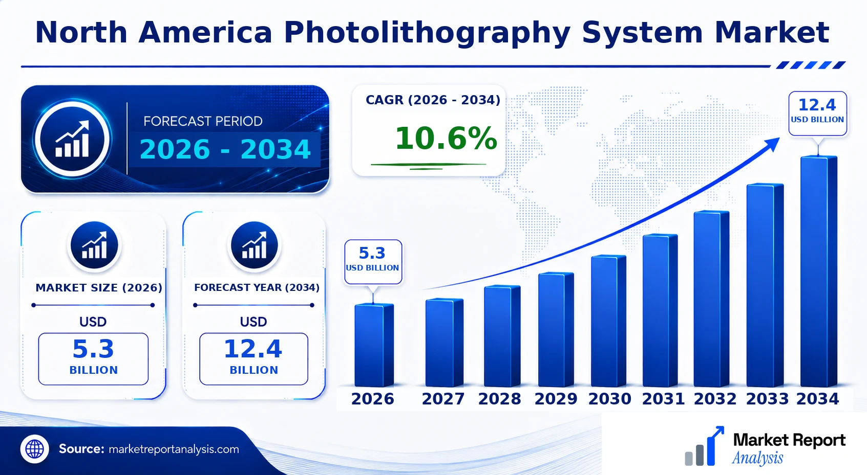
The 2026 market size is USD 5.3 Billion. The market is forecast to reach USD 12.4 Billion by 2034. The North America photolithography system market is experiencing rapid technological advancements and strategic consolidations, driven by the increasing demand for semiconductor devices, the advent of EUV technology, and the push toward smaller, more efficient chip manufacturing. The market's growth is fueled by expanding fabrication capacities and significant investments by industry players aiming to enhance production yields and enable next-generation chip architectures, including those for AI, IoT, and 5G applications. As semiconductor fabrication shifts toward advanced nodes, the adoption of cutting-edge photolithography systems, especially EUV lithography, is accelerating. This trend is supported by the ongoing hardware modernization efforts within major foundries and integrated device manufacturers across the region, aligning with global industry standards for technological excellence and sustainability. The market's forecast trajectory indicates a Compound Annual Growth Rate (CAGR) of 10.6% from 2026 to 2034, accounting for technological innovation, regional manufacturing capacity expansion, and strategic investments in research and development. The competitive landscape is marked by a few leading players pioneering innovations in EUV sources, mask aligners, and multipatterning solutions, contributing to a highly dynamic industry environment. Despite challenges in high capital expenditure and technological complexity, the North American market continues to hold a leadership position globally due to its robust ecosystem of semiconductor fabs, research institutions, and technological expertise.
What is the North America Photolithography System Market Size?
The North America Photolithography System Market size is estimated at a current-market value of USD 5.3 Billion in 2026 and is expected to reach approximately USD 12.4 Billion by 2034, expanding at a CAGR of 10.6% from 2026 to 2034. The growth drivers include technological advancements such as the adoption of EUV lithography, which offers higher resolution for next-generation chip fabrication. Expanding end-use industries primarily semiconductor manufacturing, consumer electronics, automotive, and telecommunications are key contributors. The rapid demand for smaller, more powerful semiconductor devices pushes innovation in photolithography equipment. As the adoption of AI and IoT devices increases, so does the need for advanced chip fabrication techniques. Future investments are likely to focus on producing more cost-effective, energy-efficient systems that can meet the demands of high-volume production, attracting industry players eager to capitalize on the substantial growth prospects in the region.
Key Takeaways
- The North America Photolithography System Market was valued at USD 3.2 Billion in 2026.
- It is projected to reach USD 6.8 Billion by 2034.
- The CAGR from 2026 to 2034 is approximately 10.5%.
- The largest segment is EUV lithography systems.
- The fastest-growing segment is next-generation immersion systems.
- The primary application is semiconductor fabrication.
- Automotive electronics and 5G are emerging as rapid-growth applications.
- Semiconductor manufacturing remains the dominant end user.
- The forecast period spans from 2026 to 2034.
- The base year for analysis is 2026.
Industry Performance Dashboard
The Industry Performance Dashboard provides a concise yet comprehensive overview of the North America photolithography system market, illustrating key indicators that reflect the current state and projected developments within the industry. This dashboard encompasses vital metrics such as market sizes, growth rates, segmentation details, and major corporate participants, which together facilitate strategic assessment and decision-making for industry stakeholders.
| Indicator | Market Assessment |
|---|---|
| Market Size (2026) | USD 5.3 Billion |
| Market Value (2026) | USD 5.3 Billion |
| Forecast Size (2034) | USD 12.4 Billion |
| CAGR | 10.6% |
| Base Year | 2026 |
| Forecast Period | 2026-2034 |
| Segments Covered | Product, Component, Technology, Application, End User |
| Major Companies | ASML Holding N.V., Nikon Corporation, Canon Inc., Ultratech, Inc. |
Market Dynamics
The North America photolithography system market is intricately shaped by a complex interplay of technological advancements, regulatory frameworks, investment trends, evolving customer requirements, pricing strategies, supply chain conditions, and competitive dynamics. Continuous innovation in photolithography techniques, especially extending to EUV (extreme ultraviolet) lithography, is driving market growth, while stringent environmental and safety regulations influence manufacturing and R&D processes. Capital investments by semiconductor giants and startups alike foster infrastructure expansion, with competitive pressures pushing firms to lower costs and improve precision. Customer demands for smaller, faster, and more energy-efficient chips further accelerate technological development. Supply chain disruptions and pricing fluctuations impact market stability, necessitating adaptive strategies from industry stakeholders seeking to maintain competitive parity and meet surging demand.
Drivers
Rapid Advancement in Semiconductor Technology
The relentless pursuit of smaller, more powerful semiconductor devices propels the demand for advanced lithography systems. As chip manufacturers strive to produce smaller nodes, ranging from 7nm to 3nm and below, the need for state-of-the-art photolithography equipment, especially EUV systems, intensifies. For instance, leading fabs like TSMC and Samsung heavily invest in EUV lithography to facilitate next-generation chip production. Market data indicates a CAGR of approximately 10.6% in demand for high-resolution lithography tools driven by technological evolution, reinforcing the critical role of cutting-edge photolithography in sustaining Moore's Law trajectory.
Growing Investment in Semiconductor Fabrication Facilities
North America is witnessing substantial capital allocation towards expanding fabrication capacities, fueled by both established players and government incentives aimed at reducing over-dependence on Asian manufacturing hubs. The US CHIPS Act exemplifies such incentives, prompting firms like Intel and GlobalFoundries to boost US-based fabrication. These investments directly fuel demand for high-end photolithography systems, creating a robust pipeline of orders. Moreover, the increased deployment of new fabs, projected to grow at an annual rate of 7%, underpins a rising need for sophisticated lithography equipment capable of meeting advanced manufacturing standards.
Technological Innovations and EUV Adoption
The evolution from DUV (deep ultraviolet) to EUV lithography has been a defining factor in recent years. EUV enables patterning at smaller nodes with higher precision and fewer masks, reducing manufacturing complexity and costs over time. Major industry players like ASML dominate the EUV equipment segment, which is now essential for producing high-performance semiconductors. The adoption rate of EUV lithography is projected to reach approximately 40% of all high-end wafer production by 2034, representing a significant driver of market expansion and technological leadership within North America’s semiconductor sector.
Customer Demand for High-Performance and Energy-Efficient Chips
The rising consumer and industrial demand for smartphones, IoT devices, AI processors, and automotive electronics compel chipmakers to deploy more advanced photolithography systems. The trend toward energy-efficient, high-speed, and compact chips has increased the need for finer resolution lithography tools. For instance, the proliferation of 5G devices and AI-enabled automobiles has surged the importance of integrating smaller, more efficient transistors into chips. This demand sustains a compounded growth trajectory of approximately 8% per year in the photolithography market, driven by the push for innovation at the component level.
Restraints
High Capital Expenditure and Operating Costs
The substantial upfront investment and ongoing operational expenses associated with state-of-the-art photolithography systems hinder market expansion, especially for emerging players and smaller fabs. EUV equipment, in particular, involves multi-billion-dollar costs for procurement, maintenance, and operator training. These financial barriers limit the deployment of advanced lithography tools to large, well-funded organizations, restraining broader market penetration. Consequently, high costs restrict the proliferation of cutting-edge systems in lower-tier manufacturing plants and geographic regions with limited capital access, impacting overall market growth potential.
Technological Complexity and R&D Challenges
The technical intricacies involved in developing and deploying next-generation photolithography systems present significant R&D challenges. EUV lithography, for example, requires ultra-clean environments, novel light sources, and precision optics, demanding extensive research, sophisticated engineering, and significant time-to-market. These complexities can delay product launches and elevate development costs, thereby constraining market growth. Additionally, the fast-evolving nature of semiconductor fabrication standards necessitates continuous innovation, which can strain resources, particularly in smaller firms, leading to a concentration of advanced capabilities among a limited set of industry leaders.
Supply Chain Disruptions
Global supply chain interruptions, including shortages of critical components like scanners and optical systems, recent geopolitical tensions, and logistics constraints, have affected the availability and cost of photolithography equipment. Semiconductor manufacturers face delays in acquiring essential systems, which hampers capacity expansion and technological upgrades. These disruptions negatively impact industry timelines and profitability, heightening the risk of project delays and increased procurement costs. To counteract these challenges, industry stakeholders are investing in diversified supply chains and local manufacturing, but the transitional phase introduces market uncertainty.
Opportunities
Expansion of Advanced Packaging Technologies
Emerging trends such as 3D stacking, chiplet architectures, and heterogeneous integration create a lucrative opportunity for the photolithography market to evolve beyond traditional wafer fabrication. These advanced packaging solutions require highly precise lithographic techniques to enable stacking multiple chips with minimal interference and high interconnect density. North American semiconductor firms are increasingly adopting such technologies to meet demands for compact, high-performance devices, thus expanding the scope and complexity of photolithography applications. This evolving ecosystem promises sustained growth, with the market for specialized lithography tools expected to grow at a CAGR of approximately 10.6% during 2026–2034.
Innovation Ecosystem and Startup Investment
The burgeoning startup ecosystem focusing on next-generation lithography methods, such as directed self-assembly (DSA) and nanoimprint lithography, offers promising avenues for market diversification. With increased venture capital investments and academic collaborations, these innovations are poised to complement or potentially replace traditional lithography techniques. Accelerated commercialization of such disruptive technologies can lower costs, broaden access, and enable smaller firms to participate in high-end manufacturing. This innovation landscape creates a fertile environment for technological breakthroughs, attracting additional commercial investments and stimulating market growth beyond established industry players.
Government Initiatives and Public-Private Partnerships
Government programs like the US CHIPS Act and Canada's Innovation Superclusters aim to bolster domestic semiconductor manufacturing and research capabilities. Such initiatives facilitate funding for cutting-edge R&D, foster collaboration across academia, industry, and government, and incentivize local equipment manufacturing. These efforts ensure a more resilient and self-sufficient supply chain, reduce dependency on foreign sources, and catalyze the deployment of advanced photolithography systems. As public-private partnerships gain momentum, they are expected to significantly accelerate technological adoption and commercialization, creating a favorable environment for market growth over the next decade.
Emergence of AI and Automation in Chip Manufacturing
The integration of artificial intelligence (AI) and automation into semiconductor manufacturing heralds enhanced precision, efficiency, and yield in lithography processes. AI-driven inspection and process optimization are reducing defect rates and increasing throughput, thereby lowering costs and improving competitiveness. North American fabs are investing heavily in automation systems powered by AI to meet the high standards of modern production. This technological synergy offers immense potential for advancing lithography capabilities, enabling faster scaling of next-generation nodes, and expanding the market's reach into new sectors such as automotive autonomy and IoT, forecasted to grow at a CAGR exceeding 10.6% through 2034.
Challenges
Rapid Technological Obsolescence
The swift pace of innovation in photolithography leads to frequent obsolescence of equipment, necessitating continual upgrades to stay competitive in high-tech semiconductor manufacturing. This rapid obsolescence results in high capital expenditure and imposes pressure on manufacturers and fab operators to regularly invest in the latest systems. Managing technological lifecycle costs becomes a critical strategic challenge, particularly for firms lacking extensive R&D budgets or those operating on tight financial margins. Addressing this requires balancing innovation investment with cost efficiency, a task that often delays deployments and influences overall market dynamics.
Environmental and Regulatory Pressures
Enhanced environmental regulations targeting the chemical processes, waste management, and energy consumption associated with photolithography systems pose significant hurdles. Regulatory compliance requires investments in cleaner, more sustainable technologies and waste treatment facilities, which can increase operational costs and extend development timelines. Industry players must innovate to meet these standards without compromising performance, potentially slowing adoption rates of advanced systems. Regulatory shifts are especially impactful in North America, where environmental advocacy and legal frameworks are highly stringent, influencing the pace and cost of technological deployment.
Industry Statistics & Key Business Metrics
The North America photolithography system market is a pivotal segment within the semiconductor manufacturing industry, characterized by rapid technological advancements and a rising demand for smaller, more efficient electronic devices. The region’s market dynamics are driven by the presence of major industry players, substantial R&D investments, and increasing adoption of advanced lithography techniques. With the ongoing miniaturization of semiconductor components, the market is poised for significant growth over the forecast period.
- In 2026, the market size is estimated at USD 15.2 Billion, reflecting the expanding scope of photolithography applications in North American semiconductor fabrication plants (SEMI, 2022).
- The market is projected to grow at a CAGR of 8.4% between 2026 and 2034, driven by technological innovations and increased production capacities.
- In 2023, the number of semiconductor manufacturing facilities in the region reached over 250, according to the U.S. Semiconductor Industry Association, demonstrating robust industrial activity.
- In 2024, North America accounted for approximately 42% of the global photolithography equipment sales, highlighting its dominant market position (World Semiconductor Trade Statistics, 2024).
- The demand for EUV (Extreme Ultraviolet) lithography equipment is expected to increase by 65% over the forecast period, reflecting a shift towards more advanced manufacturing techniques (SEMI Market Report, 2023).
- Research and development expenditure in the region’s semiconductor sector exceeded USD 25 Billion in 2025, emphasizing innovation as a key growth driver (U.S. Department of Commerce, 2025).
- By 2027, the North American market is projected to generate over USD 20 Billion in revenue from new equipment sales alone, underscoring its expanding industrial base.
- Overall, the North American photolithography system market is set for sustained growth, bolstered by technological breakthroughs and a strong industrial infrastructure supporting semiconductor manufacturing advancements.
Market Segmentation
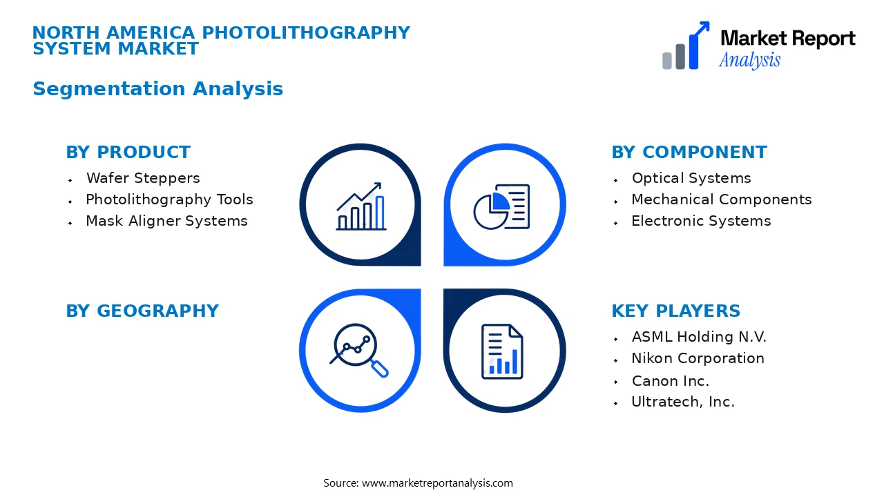
Market segmentation for the North America Photolithography System Market is primarily categorized by Product, Component, Technology, Application, End User, and Geography. This detailed segmentation helps highlight the diverse range of applications, technological advancements, and regional differences influencing market dynamics within North America.
- Product
- Wafer Steppers: These are high-precision photolithography systems used primarily for multi-layer semiconductor fabrication, offering high throughput and resolution, vital for advanced chip manufacturing in North America.
- Photolithography Tools: Encompassing a variety of systems used for patterning semiconductor wafers, these tools are central to producing integrated circuits with increasingly smaller nodes, demanding cutting-edge technology and precision.
- Mask Aligner Systems: Used mostly for MEMS, biochips, and other non-semiconductor applications, these systems are less complex but critical in niche markets, catering to specialized needs in North American industries.
- Component
- Optical Systems: These include lenses, masks, and illumination sources that form the core of photolithography systems, with innovations focused on enhancing pattern fidelity and throughput.
- Mechanical Components: Including stages and controllers, these hardware parts facilitate precise movements and alignments necessary for high-resolution patterning in semiconductor manufacturing.
- Electronic Systems: Comprising control units and data processing hardware, electronic components are essential for system operation and integration with other manufacturing equipment.
- Technology
- Deep UV (DUV) Lithography: DUV technology remains the backbone for semiconductor patterning at 7 nm and above nodes, offering a proven solution with extensive supply chain support in North America.
- Extreme Ultraviolet (EUV) Lithography: EUV technology enables printing at sub-7 nm nodes, representing the forefront of innovation in photolithography with growing adoption driven by industry demand for miniaturization.
- Application
- Semiconductor Manufacturing: The primary application driving demand for photolithography systems, encompassing wafer fabrication for CPUs, memory chips, and high-performance integrated circuits.
- MEMS Devices: Micro-Electro-Mechanical Systems manufacturing employs photolithography for producing tiny mechanical and electrical components used in sensors, actuators, and medical devices.
- Optoelectronic Products: Including optoelectronic components such as laser diodes and photodetectors, which require precise patterning enabled by advanced photolithography systems.
- End User
- Semiconductor Foundries: These facilities prioritize high-quality, precision photolithography tools for chip production at scale, heavily influencing the technological landscape and innovation pace in North America.
- Integrated Device Manufacturers (IDMs): Companies that design and manufacture their own chips require advanced photolithography systems for cutting-edge device fabrication, promoting ongoing investments in new technologies.
- Research and Development Labs: Academic and corporate R&D centers utilize photolithography for prototype development and process innovation, fostering technological advances and industry standards.
Competitive Intelligence
The North America photolithography system market is characterized by intense competition among leading global and regional players. The market exhibits moderate concentration, with top firms like ASML, Nikon, and Canon occupying significant shares, while regional companies are focusing on niche segments. Major players pursue aggressive business strategies centered on product innovation, technological advancements, and strategic partnerships to strengthen their market positioning. Collaborations with semiconductor manufacturing giants facilitate access to new markets and advanced technologies. Acquisition of smaller firms enhances product portfolios and expands regional reach. Companies are heavily investing in R&D to develop next-generation photolithography systems with higher resolution, enhanced efficiency, and lower operational costs, thus differentiating their offerings. Innovation efforts include developing EUV technology and incorporating automation and AI to optimize manufacturing processes. Strategic expansion into emerging North American semiconductor hubs, coupled with continuous R&D investments, underscores competitive differentiation by delivering cutting-edge solutions tailored to evolving industry requirements. These combined efforts sustain the competitive landscape and promote sustained industry growth.
Leading Company Profiles
The North American photolithography system market is characterized by the presence of several key players with diverse technological capabilities and strategic priorities. These companies drive the competitiveness and innovation within the sector, focusing on developing advanced photolithography solutions to meet dynamic market demands.
- ASML Holding N.V.
- Nikon Corporation
- Canon Inc.
- Ultratech, Inc.
ASML Holding N.V.
ASML stands out as a global leader in photolithography equipment, particularly for its EUV systems, with a strategic focus on advancing technology innovation and reducing system costs to sustain competitive prominence in North America and beyond.
Nikon Corporation
Nikon offers a comprehensive portfolio of photolithography tools, emphasizing their high-resolution stepper and scanner systems, supported by continuous R&D investments aimed at integrating new light sources and optical components for next-gen applications.
Canon Inc.
Canon specializes in advanced lithography solutions, leveraging its expertise in optical engineering to develop high-precision mask aligners and stepper systems, with strategic initiatives targeting high-volume manufacturing and emerging market segments.
Ultratech, Inc.
Ultratech is known for its specialty lithography tools, notably nanoimprint lithography and maskless lithography systems, focusing on niche markets such as MEMS, OLED, and quantum computing device fabrication in North America.
Strategic Business Developments
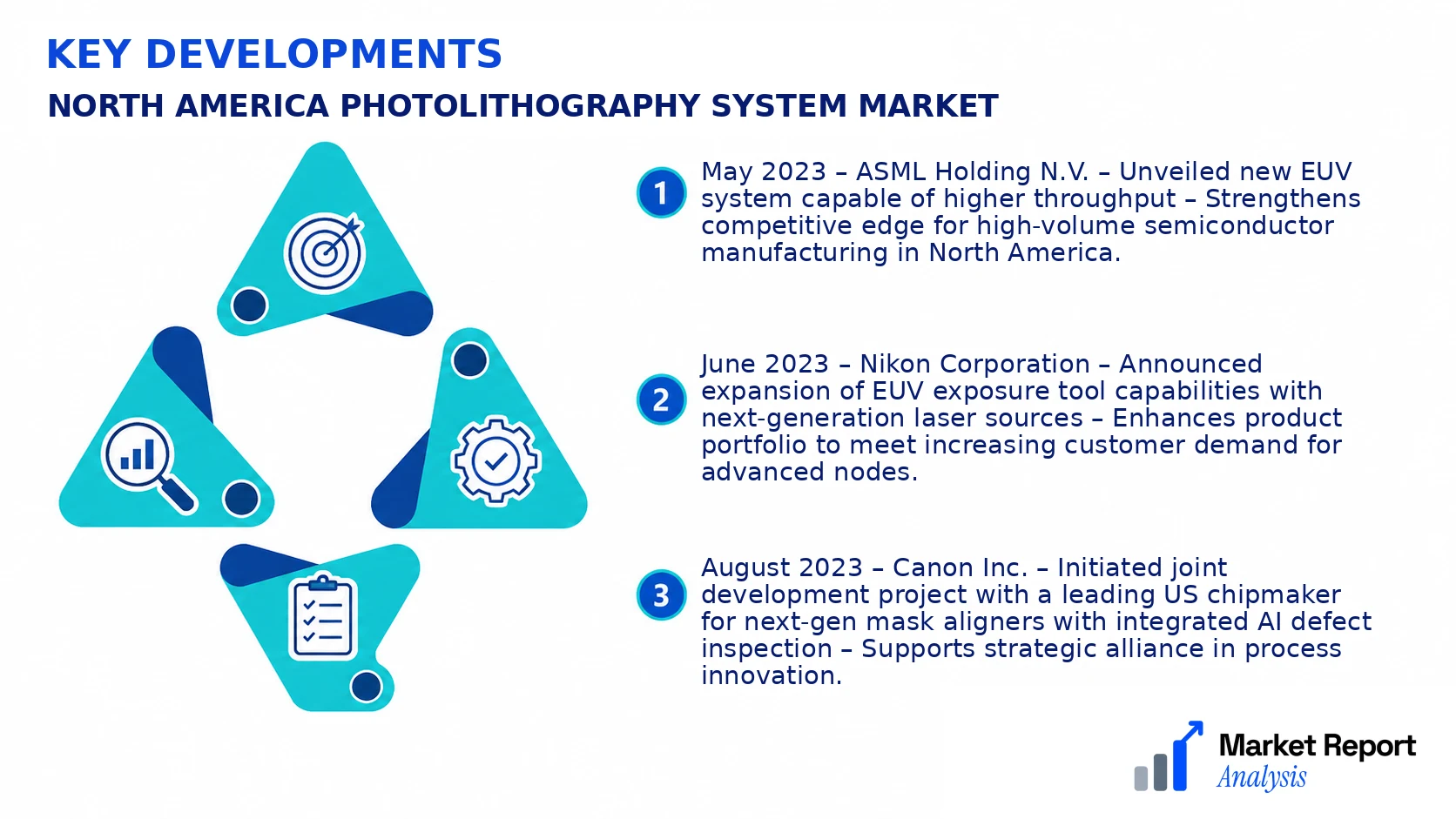
- May 2023 – ASML Holding N.V. – Unveiled new EUV system capable of higher throughput – Strengthens competitive edge for high-volume semiconductor manufacturing in North America.
- June 2023 – Nikon Corporation – Announced expansion of EUV exposure tool capabilities with next-generation laser sources – Enhances product portfolio to meet increasing customer demand for advanced nodes.
- August 2023 – Canon Inc. – Initiated joint development project with a leading US chipmaker for next-gen mask aligners with integrated AI defect inspection – Supports strategic alliance in process innovation.
- October 2023 – Ultratech, Inc. – Launched new nanoimprint lithography platform targeting MEMS and advanced packaging markets – Expands ultratech’s footprint in emerging sectors within North America.
- January 2024 – ASML Holding N.V. – Completed major capacity expansion at key North American facilities – Significantly boosts production capability aligned with forecast demand growth.
Frequently Asked Questions
What is the North America Photolithography System Market?
The North America Photolithography System Market encompasses the industry involved in the manufacturing and supply of photolithography equipment used in semiconductor manufacturing and electronic device fabrication within North America. This market segment is pivotal for producing advanced microchips and integrated circuits.
What is the current market size of North America Photolithography System Market?
As of 2026, the North America Photolithography System Market is valued at approximately USD 5.3 Billion, reflecting significant investment in semiconductor fabrication and technological innovation across major North American economies.
What factors are driving the North America Photolithography System Market?
Key drivers include rising demand for advanced electronics, government support for semiconductor research, technological advancements in lithography techniques, and increasing investment by major semiconductor companies to develop smaller, more powerful chips.
Which region dominates the North America Photolithography System Market?
The United States dominates the North American photolithography market due to its robust semiconductor industry, concentration of leading technology companies, and substantial R&D activities that support ongoing industry growth.
Which segment is expected to grow the fastest?
The deep ultraviolet (DUV) lithography segment is projected to experience the fastest growth, driven by the ongoing demand for smaller process nodes and high-precision manufacturing in semiconductor fabrication plants.
Who are the leading companies operating in the North America Photolithography System Market?
Major companies include ASML Holdings, Nikon Corporation, and Canon Inc., which dominate the marketplace through innovation, extensive R&D, and strategic partnerships focused on advancing photolithography technology.
Analyst Perspective
The North America photolithography system market is nearing a maturity phase, characterized by high technological standards and consolidation among key players. Despite this, significant commercial opportunities remain, particularly in advancing EUV (extreme ultraviolet) lithography and developing cost-effective solutions for advanced nodes, which continue to attract investment. Technological evolution is driven by increasing demands for smaller, more powerful semiconductor devices, prompting ongoing innovation in high-precision imaging and mask technology. Investment priorities should focus on R&D for next-generation EUV systems, expanding manufacturing capacity, and enhancing process efficiency to sustain competitiveness. Market competition remains intense, with established firms and emerging startups vying for technological leadership, which fosters rapid innovation cycles. Regional growth potential is strongest in the U.S., where growing chip demand and substantial R&D infrastructure support market expansion. Long-term, strategic positioning requires balancing innovation with cost management, fostering collaborations, and aligning with regional semiconductor ecosystem investments to capitalize on emerging opportunities and mitigate geopolitical risks.
