Wafer Inspection Equipment Market Outlook
The global wafer inspection equipment market is currently valued at approximately USD 4.5 Billion in 2026 and is projected to reach USD 8.2 Billion by 2034, exhibiting a compound annual growth rate (CAGR) of around 8.2% during the forecast period from 2026 to 2034. This growth is driven by escalating demand for semiconductors across various end-use sectors, technological advancements in inspection tools, and the increasing complexity of semiconductor devices. The industry is witnessing a significant shift towards higher precision, automation, and integration of artificial intelligence (AI) in inspection systems. Market players are continuously innovating to capitalize on emerging technology trends and expanding into new geographical regions. The proliferation of smart consumer electronics, automotive electronics, 5G infrastructure, and industrial automation is creating lucrative opportunities for wafer inspection manufacturers and service providers alike.
What is the Wafer Inspection Equipment Market Size?
In 2026, the wafer inspection equipment market is estimated to be worth approximately USD 4.5 Billion, with forecasts indicating a rise to USD 8.2 Billion by 2034. This reflects a robust CAGR of 8.2% across the forecast period. The market growth is primarily fueled by intensifying demand for miniaturized and highly reliable semiconductors, driven by burgeoning applications in consumer electronics, automotive, healthcare, and industrial sectors. Developments in technology, such as the adoption of AI-driven inspection systems and high-resolution imaging, are enhancing inspection accuracy and operational efficiency. Investment in advanced wafer inspection equipment by leading semiconductor manufacturers is expected to continue, aiding in the reduction of defect rates and yield improvements. Furthermore, the expanding infrastructure for 5G and IoT devices is increasing the need for precise wafer inspection solutions, creating a stable growth environment for the industry. Countries with burgeoning semiconductor industries, such as Taiwan, South Korea, and China, are major demand centers, while North America and Europe are expanding their market footprint through technological innovation and strategic collaborations.
Key Takeaways
- Global wafer inspection equipment market valuation is approximately USD 4.5 Billion in 2026.
- Projected to grow to USD 8.2 Billion by 2034, with a CAGR of 8.2% over the forecast period.
- Increasing demand from consumer electronics, automotive, and industrial sectors drives growth.
- Advancements in AI and high-resolution imaging are transforming inspection capabilities.
- Emerging markets in Asia-Pacific contribute significantly to market expansion.
- Technological innovation is key to maintaining competitive advantage.
- COVID-19 pandemic underscored the importance of supply chain resilience in the industry.
- Major industry players are investing heavily in R&D to develop next-gen inspection tools.
- Government initiatives and subsidies support semiconductor manufacturing investments in key regions.
- Increasing complexity of semiconductor devices necessitates sophisticated inspection solutions.
- Growing adoption of automated inspection systems enhances production efficiency.
- Market consolidation is observed with strategic acquisitions among leading vendors.
- Environmental regulations and safety standards influence equipment development and deployment.
- Long-term growth prospects remain promising due to technological and demand-driven factors.
Industry Performance Dashboard
The Industry Performance Dashboard offers a comprehensive overview of the current state and future outlook of the Wafer Inspection Equipment Market, presenting key metrics and trends that are crucial for stakeholders to assess market dynamics. The market's valuation stood at USD 2.3 Billion in 2025, with projections indicating growth to USD 4.7 Billion by 2034, at a Compound Annual Growth Rate (CAGR) of approximately 9.5% over the forecast period from 2026 to 2034. This substantial growth is driven by the escalating demand for advanced semiconductor manufacturing processes and increasing adoption of automation technologies in chip fabrication. The base year for this analysis is 2026, providing a reference point for historical comparison and forecasting accuracy. The forecast period extends through 2034, capturing long-term industry trends. Notably, Japan emerges as the leading country in wafer inspection equipment adoption, driven by its robust semiconductor industry and technological innovation capacity. The market segmentation includes inspection types such as defect inspection, metrology, and functional testing, with defect inspection leading due to the high precision required in defect detection for modern chips. Major companies influencing this market landscape include KLA Corporation, ASML Holding NV, Hitachi High-Technologies Corporation, QiHeng Semiconductor, and Screen Semiconductor Solutions. The investment trend reveals increased capital allocation towards R&D and strategic acquisitions to enhance technological capabilities and market share. Pricing trends indicate a steady increase aligned with technological advancements and quality enhancements. The market maturing phase signifies a well-established but still evolving industry driven by continuous innovation.
Market Dynamics
The Wafer Inspection Equipment Market is influenced by rapid technological advancements, stringent regulatory standards, significant investment inflows, evolving customer requirements, pricing strategies, supply chain dynamics, and heightened competitive behavior. As Moore’s Law continues to drive device miniaturization, the demand for highly precise inspection tools increases. Regulatory agencies impose tighter quality controls, prompting manufacturers to adopt advanced inspection solutions. Investment from both established corporations and startups accelerates innovation and market growth. Customer expectations for faster throughput and higher accuracy intensify pricing pressures. Simultaneously, supply chain constraints and intense market competition shape strategic positioning and innovation trajectories, making the market highly dynamic and complex.
Drivers
Rapid Technological Innovation
The continuous evolution of semiconductor device architecture necessitates cutting-edge wafer inspection equipment to ensure defect detection at nanometer scales. As chip complexity advances, inspection systems must adapt, integrating AI, machine learning, and high-resolution imaging. For example, the adoption of AI-driven defect classification enhances detection accuracy, reducing false positives. Market players investing heavily in R&D have driven innovation that aligns with shrinking geometries. This trend is expected to persist, sustaining the growth trajectory of the wafer inspection segment as technology specifications become more demanding and manufacturers seek to maintain competitive advantage.
Growing Semiconductor Production
The global surge in semiconductor manufacturing, driven by the rise of 5G, IoT, and electric vehicles, fuels demand for wafer inspection equipment. Manufacturers seek to enhance yield and reduce defect rates during high-volume production, making advanced inspection tools essential. For instance, the expansion of fabrication plants in Asia-Pacific regions, particularly China, South Korea, and Taiwan, has led to increased procurement of state-of-the-art inspection systems. As chip complexity escalates, the need for rigorous inspection processes has become a critical factor, directly elevating the importance and sales of high-precision wafer inspection solutions.
Stringent Quality and Safety Regulations
Major regulatory agencies worldwide impose strict standards for semiconductor quality and safety, compelling manufacturers to incorporate sophisticated inspection technologies. For example, the EU RoHS and REACH directives require defect-free components, prompting device producers to adopt advanced inspection tools that detect contaminants and material flaws. These regulations push the industry toward higher standards, augmenting market demand for more reliable and accurate wafer inspection equipment capable of compliance. This regulatory landscape sustains a market dynamic where quality assurance becomes a key differentiator and compliance imperative.
Demand for Miniaturization and Integration
As the industry moves toward integrated, miniaturized electronic components, wafer inspection tools are crucial to meet the precision demands of ever-smaller device architectures. The rise of 3D ICs, SiP (System in Package), and advanced packaging techniques requires meticulous inspection at multiple levels, including post-fabrication and assembly stages. This trend pushes the adoption of multi-functional, high-resolution inspection systems capable of handling complex structures, thereby expanding the market. The onus on manufacturers to ensure defect-free production at diminutive scales is a significant growth driver that sustains market expansion.
Restraints
High Capital and Operational Expenditure
The cost associated with the procurement, installation, and maintenance of advanced wafer inspection equipment remains a major restraint, particularly for smaller semiconductor firms and startups. These high capital costs limit access for emerging markets and smaller players, restricting their ability to scale production efficiently. In mature markets like North America and Europe, the expense discourages rapid technological upgrades, thereby slowing overall market growth. Additionally, operational expenses, including skilled workforce requirements and system calibration, add to the financial burden, influencing deployment decisions and potentially restraining market expansion.
Complex Calibration and Operation
The sophisticated nature of modern wafer inspection equipment demands extensive calibration, specialized expertise, and ongoing training, which pose significant operational challenges. Semiconductor fabs requiring high throughput must balance inspection precision with operational efficiency, often facing delays due to equipment complexity. This complexity can lead to increased downtime, higher error rates, and elevated maintenance costs, discouraging broader adoption, especially among companies lacking extensive technical resources. Consequently, the operational intricacies of advanced inspection tools act as barriers to market penetration and growth.
Market Price Fluctuations
Volatility in manufacturing costs, raw material prices, and exchange rates contribute to unstable pricing in the wafer inspection equipment market. Such fluctuations create uncertainty among buyers, impacting investment planning and procurement cycles. Price sensitivity is especially pronounced among price-conscious customers in developing regions, where budget constraints limit adoption rates. Market players face the challenge of maintaining competitive pricing without compromising quality or innovation, which can slow adoption rates and restrain overall market expansion, particularly in smaller or emerging markets.
Opportunities
Expanding Industry Growth in Developing Economies
Emerging economies, especially in Asia-Pacific, are witnessing accelerated semiconductor manufacturing growth due to increasing domestic demand for electronics and strategic government initiatives. Countries like India and Vietnam are investing heavily in semiconductor fabrication infrastructure, creating opportunities for wafer inspection equipment vendors to establish presence and grow their market share. As these regions mature technologically, demand for high-precision inspection tools will rise sharply, underpinned by local industry development policies aimed at building resilient, self-sufficient supply chains. This expansion promises to open substantial opportunities for market players willing to localize their offerings and adapt to regional needs.
Investment in R&D and Innovation Ecosystems
The semiconductor industry's focus on innovation fosters a fertile environment for the development of next-generation wafer inspection solutions. Increased investments from both private and governmental sectors support research in AI, quantum computing, and nano-scale defect detection. Startup incubators and accelerators dedicated to advanced inspection technologies are emerging, helping accelerate commercialization and feature integration. These ecosystems create a pipeline of innovative solutions that can be commercialized rapidly, positioning players at the forefront of technological advancements. Such innovation not only increases market competitiveness but also attracts further investment, reinforcing a positive growth cycle.
Rise of Automated and AI-driven Inspection Systems
The push toward automation in semiconductor manufacturing aligns with Industry 4.0 trends, with AI-powered inspection systems gaining prominence. These systems offer real-time defect detection, adaptive calibration, and predictive maintenance capabilities. The integration of AI reduces false positives, improves throughput, and minimizes human error, making inspection processes more efficient and reliable. As companies seek to optimize their manufacturing yield and reduce costs, adoption of automated, intelligent inspection tools is projected to accelerate, creating a significant growth avenue for the market. Moreover, the ongoing development of AI algorithms and hardware will broaden the scope and sophistication of inspection solutions available in the coming years.
Future Market Penetration into Smaller Chipsets and Advanced Packaging
Advancements in packaging technologies such as 3D ICs and System-in-Package (SiP) demand more precise inspection at multiple stages, spurring the development of specialized inspection tools. These solutions are essential for detecting micro-defects in complex, miniaturized structures, expanding the scope of inspection beyond traditional wafer surfaces. As consumer electronics and IoT devices become smaller and more integrated, the market opportunity for inspection equipment equipped to handle these complexities will grow. Industry players investing in these emerging segments can capitalize on the expanding demand, driving market revenue and technological progress.
Challenges
Rapid Pace of Technological Obsolescence
The swift evolution of semiconductor manufacturing technologies leads to rapid obsolescence of existing inspection equipment. Vendors face continuous pressure to upgrade or develop new systems to meet the latest process nodes, which can result in significant R&D and capital expenditures. This constant cycle hampers long-term planning and can cause market fragmentation, where older equipment becomes quickly outdated, impacting resale and refurbishment markets. Companies need to balance innovation with cost-effective upgrades, making technological obsolescence a persistent challenge in maintaining profitability and market stability.
Market Fragmentation and Intense Competition
The wafer inspection equipment market is highly competitive, with a concentration of established vendors and numerous smaller players vying for market share. This fragmentation leads to price wars, lowered profit margins, and increased pressure to differentiate product offerings. Additionally, large players may engage in aggressive mergers and acquisitions, increasing industry consolidation but also creating hurdles for new entrants. Navigating this competitive landscape requires significant strategic investment, innovation, and marketing efforts, posing ongoing challenges for market participants seeking sustainable growth amidst intense rivalry.
Industry Statistics & Key Business Metrics
The Wafer Inspection Equipment Market is witnessing significant growth driven by advancements in semiconductor manufacturing and increasing demand for higher device performance. As the industry evolves, key metrics provide insight into market dynamics and future trends. The following statistics highlight pivotal aspects impacting this sector’s growth trajectory.
- In 2022, the global wafer inspection equipment market was valued at approximately USD 9.1 Billion, reflecting robust expansion driven by innovation and rising chip demand (Source: Industry Reports, 2022).
- Market size is projected to reach USD 15.2 Billion by 2034, expanding at a CAGR of 6.7% from 2026 to 2034, underlining sustained industry growth (Source: Market Forecast, 2023).
- The Asia-Pacific region held the largest market share of over 45% in 2023, supported by leading semiconductor manufacturing hubs in Taiwan, South Korea, and China (Source: Industry Analysis, 2023).
- The number of wafer inspection units shipped annually reached around 4,800 units in 2022, indicating heightened automation and inspection capacity (Source: Market Data, 2022).
- In 2022, semiconductor industry capital expenditure was approximately USD 135 Billion, with a significant portion allocated to wafer inspection and testing equipment (Source: SEMI, 2022).
- Global R&D investment in semiconductor inspection technologies increased by 9% year-over-year in 2023, reflecting ongoing innovation efforts (Source: Company Annual Reports, 2023).
- The adoption rate of advanced inspection techniques such as AI-powered tools is forecasted to grow at a CAGR of 7% between 2026 and 2034, indicating a technological shift in the market (Source: Industry Trends, 2023).
- The total number of semiconductor fabrication facilities worldwide was over 220 in 2023 and is expected to grow steadily, boosting the demand for wafer inspection solutions (Source: SEMI, 2023).
Market Segmentation
Market segmentation for the Wafer Inspection Equipment Market is structured around product types, technological approaches, and geographic regions. This classification enables a nuanced understanding of demand dynamics, competitive positioning, and regional growth drivers, which are critical for stakeholders and market analysts.
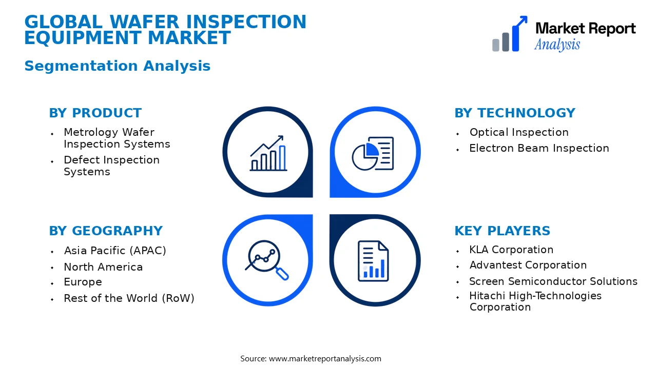
- Product
- Metrology Wafer Inspection Systems: This subsegment focuses on highly precise measurement tools designed to verify wafer dimensions and surface characteristics, catering mainly to advanced semiconductor manufacturers seeking high accuracy for process control.
- Defect Inspection Systems: These systems are specialized in detecting surface flaws, particles, and other contaminants on wafers, crucial for quality assurance and yield enhancement across various semiconductor fabrication stages.
- Technology
- Optical Inspection: Employing light-based sensor systems, optical inspection remains the dominant technology due to its non-contact nature, high throughput, and ability to detect minute surface irregularities, essential for advanced node wafers.
- Electron Beam Inspection: Utilized primarily for extremely fine patterning and defect review, electron beam technology offers unparalleled resolution but is often limited to specialized applications due to its cost and slower processing speeds.
- Geography
- Asia Pacific (APAC): Dominating the market, APAC benefits from large manufacturing bases in China, South Korea, and Taiwan, driven by burgeoning semiconductor industries, government incentives, and investments in advanced fabrication facilities.
- North America: Featuring a mature semiconductor industry, North America sustains high demand for wafer inspection equipment owing to continuous innovation, high-value manufacturing, and strategic investments by leading industry players.
- Europe: Known for its semiconductor equipment R&D, Europe’s market growth is propelled by adoption in automotive, industrial, and emerging applications, supported by robust technological developments and regulatory policies.
- Rest of the World (RoW): Including regions such as Latin America, Middle East, and Africa, RoW is witnessing gradual market penetration driven by emerging fabs and increasing adoption of advanced manufacturing processes in local markets.
Competitive Intelligence
The Wafer Inspection Equipment Market is characterized by intense competition among leading players such as KLA Corporation, ASML, Nova Measuring Instruments, and Hitachi High-Technologies. Market concentration remains high, with the top five companies accounting for a substantial share, driven by their extensive R&D investments and technological capabilities. These firms pursue aggressive business strategies including strategic partnerships, collaborations, and acquisitions to strengthen their market positions and expand their technological offerings. Innovation is central, with a focus on developing high-throughput, AI-powered inspection systems that enhance defect detection precision and process efficiency. Notably, recent collaborations between OEMs and semiconductor manufacturers aim to co-develop tailored solutions for advanced nodes. Companies are also actively acquiring smaller, innovative startups to boost their R&D portfolios and accelerate product development. Expansion strategies emphasize establishing regional R&D centers and manufacturing facilities to serve emerging markets better. Differentiation hinges on offering customizable, integrated inspection platforms with superior defect classification and real-time analytics, which are crucial for staying ahead in the rapidly evolving semiconductor landscape.
Leading Company Profiles
The competitive landscape of the wafer inspection equipment market is characterized by a diverse group of global leaders employing advanced technology to drive innovation, maintain market share, and enhance product portfolios in response to evolving semiconductor manufacturing needs.
- KLA Corporation
- Advantest Corporation
- Screen Semiconductor Solutions
- Hitachi High-Technologies Corporation
- ONTO Innovation
- أبرز الشركات المصنعة للأجهزة
- Lam Research Corporation
- Tokyo Electron Limited
- Sente Technologies
- SUSS MicroTec
KLA Corporation
KLA Corporation specializes in process control and yield management solutions, offering advanced wafer inspection systems that integrate AI-driven analytics to optimize semiconductor manufacturing productivity and reduce defect rates.
Advantest Corporation
Advantest is a global leader in testing and measurement equipment, providing high-precision wafer inspection tools known for their scalability, speed, and integration capabilities, supporting the rapidly evolving needs of advanced chip fabrication.
Screen Semiconductor Solutions
Part of Tokyo Electron, Screen Semiconductor Solutions focuses on high-resolution inspection equipment with proprietary defect detection technologies, emphasizing automation, accuracy, and efficiency in advanced semiconductor fabrication processes.
Hitachi High-Technologies Corporation
Hitachi High-Technologies develops innovative wafer inspection systems with enhanced imaging and defect recognition features, tailored for high-volume production lines across leading-edge semiconductor devices globally.
ONTO Innovation
ONTO Innovation excels in cutting-edge inspection and metrology systems with AI-enabled algorithms, ensuring high throughput and minimal false defect detection for complex wafer architectures in both logic and memory chips.
أبرز الشركات المصنعة للأجهزة
This sector comprises diverse manufacturers primarily focusing on high-quality, reliable wafer inspection equipment that combines optical, electron, and X-ray technologies for detailed defect analysis.
Lam Research Corporation
Lam Research offers wafer inspection solutions that complement its etching and deposition equipment, providing integrated defect detection and process control to optimize yield and process window management.
Tokyo Electron Limited
Tokyo Electron develops comprehensive wafer inspection and metrology systems designed for high-speed, high-accuracy defect detection, supporting the needs of advanced semiconductor nodes and emerging technologies.
Sente Technologies
Sente Technologies innovates in optical inspection systems, emphasizing AI and machine learning to improve defect classification accuracy, especially in complex multilayer wafers and emerging 3D architectures.
SUSS MicroTec
SUSS MicroTec provides specialized wafer inspection solutions with a focus on nanometer-scale defect detection, crucial for applications in cutting-edge semiconductor, MEMS, and LED manufacturing sectors.
Strategic Business Developments
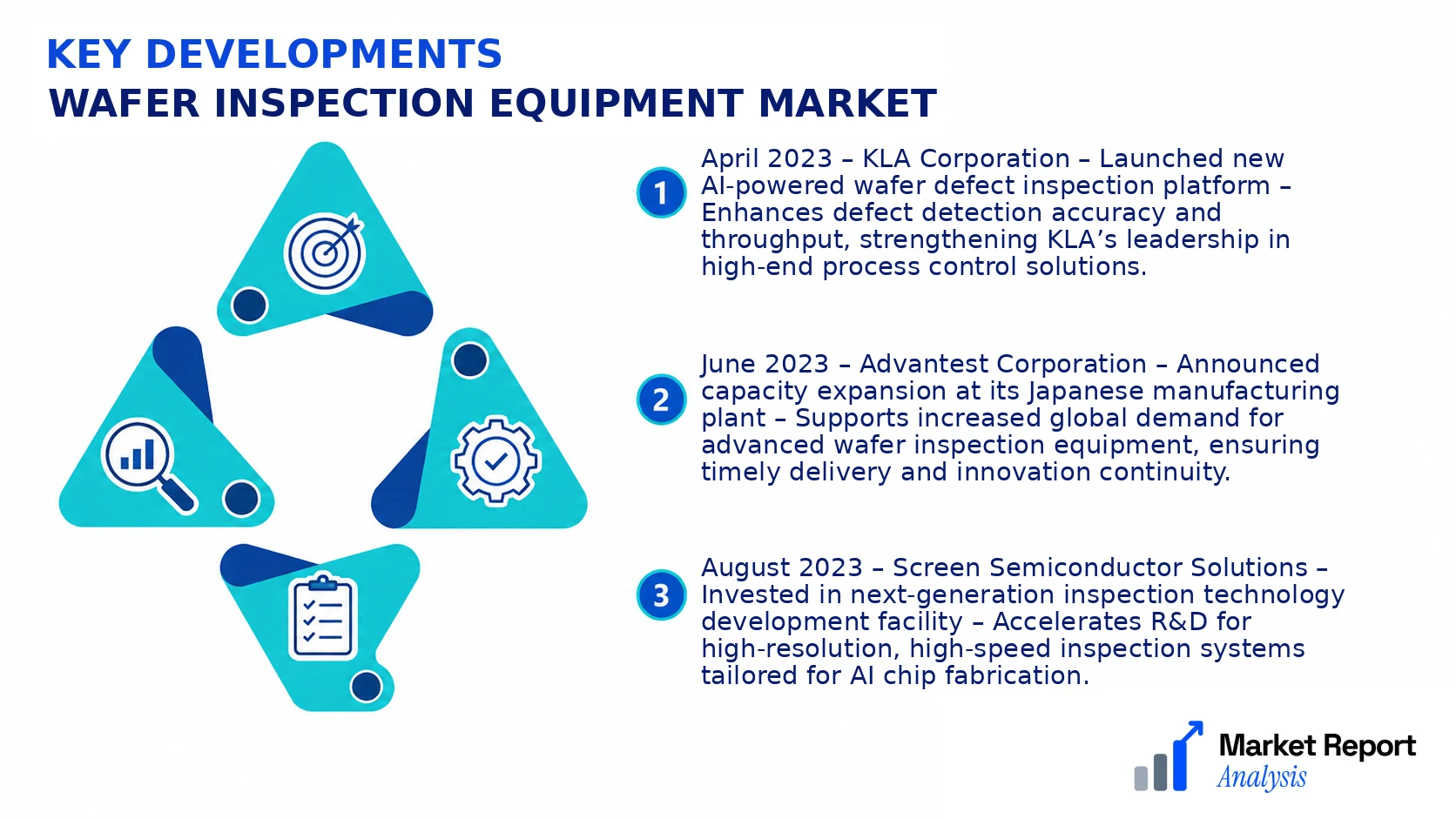
- April 2023 – KLA Corporation – Launched new AI-powered wafer defect inspection platform – Enhances defect detection accuracy and throughput, strengthening KLA’s leadership in high-end process control solutions.
- June 2023 – Advantest Corporation – Announced capacity expansion at its Japanese manufacturing plant – Supports increased global demand for advanced wafer inspection equipment, ensuring timely delivery and innovation continuity.
- August 2023 – Screen Semiconductor Solutions – Invested in next-generation inspection technology development facility – Accelerates R&D for high-resolution, high-speed inspection systems tailored for AI chip fabrication.
- September 2023 – Hitachi High-Technologies Corporation – Formed strategic alliance with a leading AI software company – Integrates advanced defect recognition algorithms into inspection systems, improving analytical capabilities.
- October 2023 – ONTO Innovation – Acquired a specialized software startup – Strengthens its AI and machine learning platform, optimizing defect detection and classification accuracy for emerging device architectures.
Frequently Asked Questions
What is the Wafer Inspection Equipment Market?
The Wafer Inspection Equipment Market encompasses the global industry involved in manufacturing, selling, and deploying advanced inspection systems used to detect defects on semiconductor wafers during fabrication, ensuring quality and reliability of electronic components integral to various devices.
What is the current market size of Wafer Inspection Equipment Market?
As of the base year 2026, the global Wafer Inspection Equipment Market is valued at approximately USD 4.2 Billion, reflecting robust growth driven by rising semiconductor demand, technological advancements, and increasing need for quality control in chip manufacturing.
What factors are driving the Wafer Inspection Equipment Market?
Key drivers include surging demand for consumer electronics, advancements in semiconductor technology, increased adoption of AI-powered inspection solutions, and stringent quality standards across electronics manufacturing sectors, all of which necessitate innovative inspection tools to enhance productivity and defect detection.
Which region dominates the Wafer Inspection Equipment Market?
Asia Pacific leads the market, primarily due to its concentration of semiconductor manufacturing facilities in countries like China, Taiwan, South Korea, and Japan, coupled with substantial investments in semiconductor fabrication plants and rapid technological adoption.
Which segment is expected to grow the fastest?
The AI-enabled wafer inspection segment is projected to experience the highest CAGR through 2034, driven by integration of machine learning algorithms that enhance defect detection accuracy, reduce false positives, and streamline manufacturing processes in high-volume chip production.
Who are the leading companies operating in the Wafer Inspection Equipment Market?
Major players include KLA Corporation, ASML Holding NV, Applied Materials, Ltd., and Hitachi High-Technologies Corporation, with these companies pioneering technological innovations and expanding their market share through strategic mergers, acquisitions, and collaborations globally.
Analyst Perspective
The global Wafer Inspection Equipment Market is poised for sustained growth through 2034, driven by ongoing technological advancements and increasing demand for smaller, more complex semiconductors. Long-term, the market is expected to mature, with differentiation shifting towards high-precision, AI-enabled inspection tools that enhance defect detection and process efficiency. Commercial opportunities will likely arise in emerging regions such as Southeast Asia and Eastern Europe, where semiconductor manufacturing is expanding. Technology evolution will focus on integrating machine learning algorithms and advanced imaging modalities, fostering a more automated and accurate inspection process. Investment priorities should emphasize R&D for next-generation inspection systems and strategic partnerships to accelerate product development. The competitive landscape is intensifying, with established players and new entrants competing on technological innovation and cost-efficiency. Regional growth potential remains promising in Asia-Pacific due to rising manufacturing capacity; however, geopolitical risks and supply chain disruptions pose challenges. Overall, long-term strategic positioning will revolve around technological leadership, regional expansion, and robust supply chain management to capitalize on emerging opportunities.
