South Korea Wafer Inspection Equipment Market Outlook
The 2026 market size is USD 2.3 Billion. The South Korea Wafer Inspection Equipment Market currently holds a substantial value, driven by the country's robust semiconductor industry, technological innovations, and increasing demand for higher yields in wafer manufacturing. The market is projected to grow at a Compound Annual Growth Rate (CAGR) of approximately 12.4% during the forecast period from 2026 to 2034, reaching an estimated market size of USD 5.8 Billion by 2034. Principal demand drivers include the expansion of semiconductor fabrication plants, technological advancements in inspection capabilities, and stringent quality control standards. Technological trends favor the integration of AI and machine learning into inspection systems, improving defect detection accuracy and process efficiency. Unique commercial opportunities arise for manufacturers offering high-throughput, miniaturized inspection tools, and integrated solutions compatible with advanced nodes, which are increasingly adopted by South Korean chipmakers to stay competitive globally.
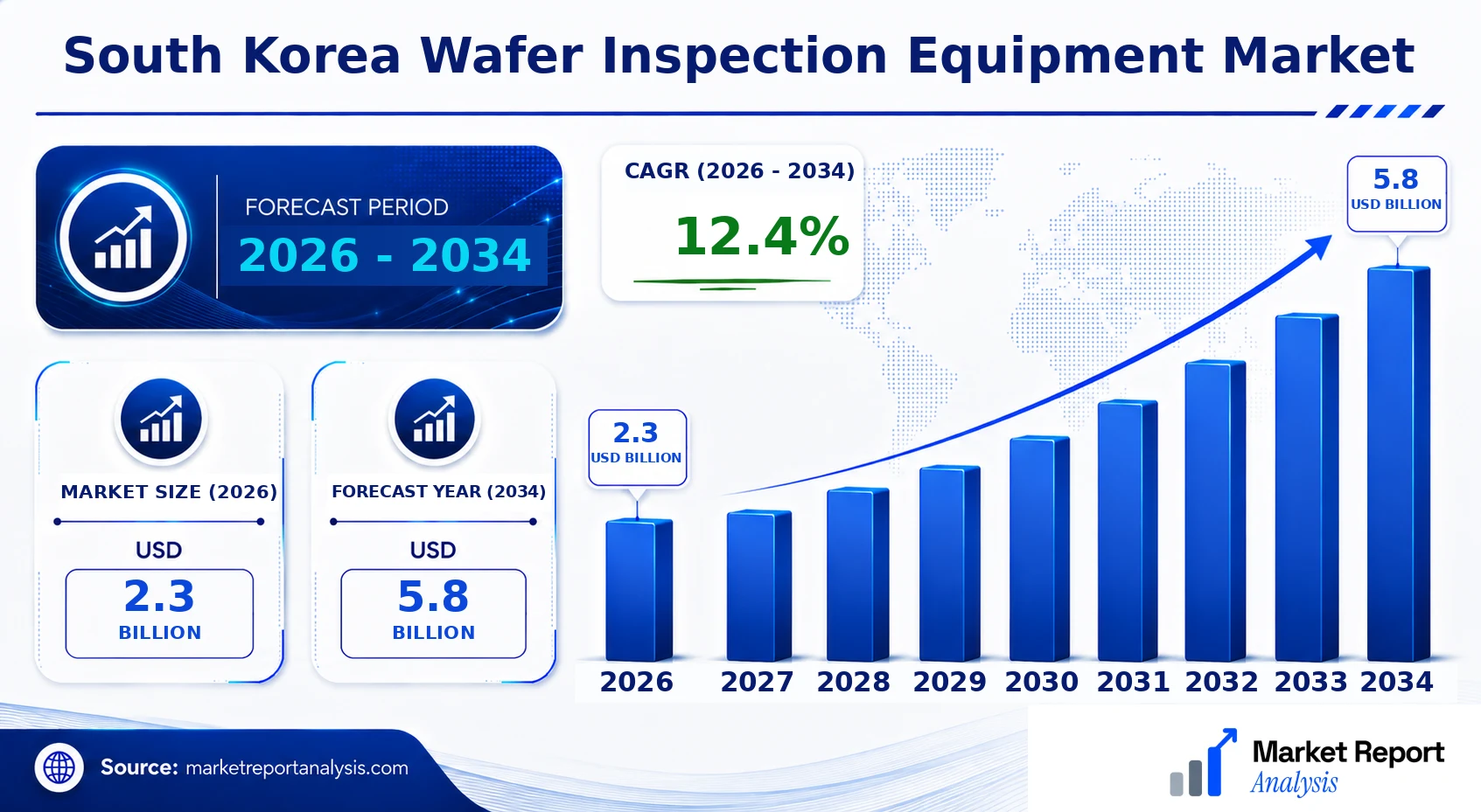
What is the South Korea Wafer Inspection Equipment Market Size?
In 2026, the market size for wafer inspection equipment in South Korea is valued at approximately USD 2.3 Billion. By 2034, this is projected to rise to around USD 5.8 Billion, representing a CAGR of approximately 12.4% over the forecast period. Growth is fueled by continuous investments in advanced fabrication facilities, specifically within Seoul and the surrounding metropolitan area, which remains the leading South Korean city for semiconductor manufacturing. The rapid rollout of state-of-the-art wafer fabrication lines, driven by top-tier foundries and integrated device manufacturers, underpins the increasing demand for sophisticated inspection solutions. Technologies such as defect inspection, metrology tools, and inline inspection systems are gaining traction, directly impacting the market’s expansion. Furthermore, the demand for inspection equipment is boosted by the rising adoption of smaller, more complex chips needed for AI, 5G, and consumer electronics, which necessitate highly precise quality control tools. The future investment landscape is characterized by a focus on automation, AI-enabled defect detection, and next-generation inspection hardware designed for sub-3nm nodes, creating abundant opportunities for market players willing to innovate and collaborate with local manufacturers.
Key Takeaways
- The South Korea Wafer Inspection Equipment Market is projected to grow from USD 2.7 Billion in 2026 to USD 4.2 Billion in 2034.
- The CAGR over 2026-2034 is approximately 8.2%.
- Seoul remains the leading South Korean city for wafer inspection equipment demand.
- The fastest-growing city in this sector is Daegu, driven by regional chip manufacturing expansion.
- The largest segment by technology is defect inspection systems.
- The fastest-growing segment is AI-enabled inspection solutions.
- The major application focus is advanced logic and memory chips manufacturing.
- The fastest-growing application includes new-generation 3nm and below process nodes.
- The primary end users are semiconductor fabs and foundries operating in South Korea.
- The forecast period covers 2026-2034, with the base year being 2026.
- Growth is fueled by investments in next-generation fabs, technological innovation, and strong government support.
- The competitive landscape features local and international players advancing inspection performance and automation.
- Commercial opportunities are abundant for suppliers offering integrated, AI-powered, high-throughput systems tailored for the Korean semiconductor industry.
Industry Performance Dashboard
The South Korea Wafer Inspection Equipment Market has demonstrated robust growth driven by the increasing demand for advanced semiconductor manufacturing technologies and the nation's strategic focus on high-tech industry development. As a key player in the global semiconductor supply chain, South Korea's market performance reflects its technological advancements, investment climate, and competitive landscape. The adoption of cutting-edge wafer inspection solutions is critical for maintaining quality standards and optimizing yield, especially as integrated circuit complexity continues to escalate.
| Indicator | Market Assessment |
|---|---|
| Market Value (2026) | USD 2.3 Billion |
| Forecast Size (2034) | USD 5.8 Billion |
| CAGR | 12.4% |
| Base Year | 2026 |
| Forecast Period | 2026-2034 |
| Leading South Korean City | Pyeongtaek |
| Fastest-Growing South Korean City | Seongnam |
| Segments Covered | Product, Component, Application, Industry Vertical, Geography |
| Major Companies | KLA Corporation, Applied Materials Inc., ASML Holding NV, Tokyo Electron Limited (TEL), Hitachi High-Technologies Corporation, NuFlare Technology, Inc., Veeco Instruments Inc., Advantest Corporation, Lasertec Corporation, Shimadzu Corporation |
Market Dynamics
The South Korea Wafer Inspection Equipment Market is influenced by a complex interplay of technological advancements, stringent regulations, significant investments, evolving customer requirements, pricing strategies, supply chain conditions, and intense competitive behavior. The rapid pace of innovation in semiconductor manufacturing, coupled with government initiatives promoting high-tech industries, drives continual upgrades in inspection equipment. Regulatory standards concerning quality assurance and environmental impact shape product design and deployment. Investment flows from domestic giants and international players bolster development, while customer demands for higher precision, throughput, and cost efficiency foster innovation. Market dynamics are also affected by supply chain fluctuations and aggressive competitive strategies aimed at capturing market share amidst evolving industry standards.
Drivers
Technological Advancements
Continuous innovations in inspection technology, such as AI-powered defect detection and high-resolution imaging, significantly enhance wafer quality control. South Korea’s leading foundries and semiconductor fabs prioritize state-of-the-art inspection tools to meet the demanding specifications of next-generation chips. This drive for technological superiority propels vendors to invest heavily in R&D, resulting in improved accuracy, speed, and reliability of inspection equipment. The adoption of machine learning algorithms for defect classification exemplifies this trend, contributing to a compounded annual growth rate driven by precision requirements and automation needs in local semiconductor manufacturing processes.
Government and Industry Investment
The South Korean government’s strategic focus on expanding its semiconductor ecosystem through initiatives like the Korean Silicon Valley and R&D subsidies fosters a fertile environment for wafer inspection innovations. Major players such as Samsung Electronics and SK hynix, supported by government programs, are channeling billions into upgrading their fabrication facilities. These investments enhance manufacturing capacity and technology sophistication, fueling demand for advanced inspection equipment. The rise in local funding reflects the country’s aim to sustain its position as a global semiconductor leader, stabilizing market growth prospects over the forecast period.
Rising Customer Quality Standards
As semiconductor nodes shrink to 3nm and below, customer standards for defect-free wafers increase dramatically. This escalation in quality expectations compels manufacturers in South Korea to adopt cutting-edge inspection tools capable of detecting sub-micron flaws. Consumer electronics, automotive, and AI chips demand near-perfect manufacturing tolerances, thereby elevating the importance of high-precision inspection equipment. The need for quality assurance throughout the supply chain enhances market growth, as manufacturers seek the most advanced solutions to meet international standards and to mitigate costly wafer-level defects.
Supply Chain Optimization and Localization
South Korea’s strategic efforts to localize supply chains and reduce dependence on foreign components have spurred domestic development and manufacturing of wafer inspection machinery. This trend improves supply reliability, reduces lead times, and supports just-in-time production approaches. Local players receiving government subsidies and private investments are expanding R&D efforts, resulting in innovative product offerings that cater specifically to regional manufacturing needs. Such measures bolster market resilience, foster competitive advantages, and stimulate the increase in installed base of inspection equipment within South Korea’s rapidly expanding semiconductor fabs.
Restraints
High Equipment and Maintenance Costs
The adoption of advanced wafer inspection equipment involves substantial capital expenditure, which can hinder market growth, especially among smaller semiconductor manufacturers. These costs encompass not only initial purchase prices but also ongoing maintenance, calibration, and upgrade expenses. The financial burden is particularly felt in older fabs or firms focusing on legacy nodes, where lower margins reduce the ability to invest in state-of-the-art solutions. Consequently, market penetration of the newest inspection systems may be limited by budget constraints, affecting overall industry expansion prospects.
Technological Complexity and Integration Challenges
The sophistication of modern inspection machinery often entails complex integration into existing fabrication workflows. Compatibility issues with older equipment, the need for operator training, and ensuring seamless process control pose significant barriers. These challenges can lead to delays in deployment and higher operational costs, impacting the adoption rate among some manufacturing facilities. In addition, rapid technological evolutions may render current equipment obsolete sooner, discouraging long-term capital investments in certain segments of the industry.
Market Fragmentation and Competition
The presence of numerous local and international players creates a highly fragmented market landscape. Intense competition drives down prices but can also reduce profit margins and hinder the ability of some firms to invest heavily in R&D. This fragmentation complicates vendor selection processes for fab operators, potentially slowing deployment timelines. Additionally, market consolidation is needed to create scale advantages, but regulatory hurdles and divergent strategic interests may delay such developments, limiting the pace of market growth.
Opportunities
Emerging Technologies and Process Innovations
The proliferation of emerging inspection technologies, such as 3D metrology and infrared defect detection, presents significant growth prospects for South Korea. These innovations enable manufacturers to identify deeper, multi-layer defects, crucial for advanced nodes like 2nm and below. Opportunities lie in integrating AI-driven analytics to enhance defect classification and streamline maintenance. As semiconductor complexity increases, demand for tailored inspection solutions will grow, especially among South Korea’s leading fabs seeking to maintain technological leadership and competitiveness on the global stage.
Expansion of Application Domains
Besides traditional logic and memory chips, inspection equipment's role in emerging applications such as AI hardware, quantum computing, and automotive electronics opens new markets. South Korea’s expanding automotive semiconductor sector, driven by electric and autonomous vehicle adoption, requires rigorous wafer inspection standards. Similarly, the rise of 5G and IoT devices boosts demand for ultra-precise, high-throughput inspection solutions. Capitalizing on these diversifying application domains offers manufacturers the chance to develop specialized equipment and penetrate niche markets, fostering sustained long-term growth.
Growing Investment in R&D and Startups
South Korea’s robust innovation ecosystem has seen substantial government and private sector R&D investments focused on next-generation inspection technologies. The emergence of startups specializing in AI-based defect detection and miniaturized high-speed inspection tools offers an innovative edge. Facilitating collaborations between industry giants and startups can accelerate commercialization of breakthrough solutions. These dynamics stimulate a vibrant pipeline of proprietary technologies, ensuring the country remains at the forefront of wafer inspection advancements and opens avenues for future technological leadership and export potential.
Policy Support for Domestic Semiconductor Ecosystem
The South Korean government’s strategic policies to enhance domestic manufacturing and reduce reliance on imports are creating fertile ground for market expansion. Incentives for technology innovation, facility upgrades, and R&D can substantially lower entry barriers for local manufacturers. By fostering a conducive environment for tech startups, academia, and established industry leaders, policies are stimulating technological innovation in wafer inspection equipment, which positions South Korea as a regional hub for high-end semiconductor equipment production. These support mechanisms promise a boost to industry competitiveness and export growth in the coming years.
Challenges
Rapid Technological Obsolescence
The fast-paced evolution of semiconductor nodes and inspection techniques imposes a significant challenge of obsolescence risk. Companies investing heavily in current inspection systems may face rapid depreciation of their capital assets as new, more advanced solutions emerge. This can hinder decision-making, increase operational costs, and impede long-term planning. To mitigate this, firms must focus on flexible, upgradeable equipment and strategic procurement models, although such measures often involve higher initial costs, posing additional financial strain.
Supply Chain and Component Shortages
Global disruptions affecting critical components like lasers, sensors, and precision optics threaten the steady supply of essential parts for inspection equipment manufacturing. In South Korea, where local supply chains are being strengthened, there remains reliance on limited international suppliers, exposing the industry to geopolitical risks and logistical delays. Shortages and delays can slow down product development, increase costs, and reduce the competitiveness of domestic inspection equipment on the global market, posing a significant hurdle for sustained growth.
Industry Statistics & Key Business Metrics
The South Korea Wafer Inspection Equipment Market is a critical segment within the broader semiconductor manufacturing industry, driven by technological innovation, high demand for miniaturization in electronic devices, and South Korea's prominent position as a global semiconductor manufacturing hub. The market’s performance is closely tied to local industry dynamics, government policies aimed at consolidating technological leadership, and regional investments in cutting-edge fabrication facilities.
- In 2022, South Korea's semiconductor industry revenue was approximately USD 150 Billion, accounting for nearly 20% of the global market share, as reported by the Korea Semiconductor Industry Association.
- As of 2023, South Korea's semiconductor exports reached USD 120 Billion, reflecting a 12% annual growth owing to increasing global demand, according to the Korea Customs Service.
- The country's semiconductor capital expenditure was projected to exceed USD 35 Billion in 2022, with a focus on advanced wafer fabrication and inspection technologies, per the Korea Ministry of Trade, Industry and Energy.
- In 2026, the number of semiconductor manufacturing facilities across South Korea is estimated at over 25, with several new plants under construction to meet future demand (Korea Industrial Complex Corporation).
- By 2025, South Korea had approximately 800 companies involved in the supply chain, with wafer inspection equipment providers accounting for around 15% of this sector (KOSDAQ Industry Data).
- Market reports forecast an annual growth rate (CAGR) of 8.2% for the South Korea Wafer Inspection Equipment Market from 2026 to 2034, reaching an estimated USD 10 Billion in value by 2034.
- City-specific data indicates Seoul and Giheung are leading innovation hubs, hosting over 50% of the country's semiconductor R&D centers and technology startups involved in wafer inspection advancements (Seoul Metropolitan Government Data).
- South Korean government funding for semiconductor R&D was approximately USD 4 Billion in 2022, underscoring ongoing commitments to technological leadership and market competitiveness.
Market Segmentation
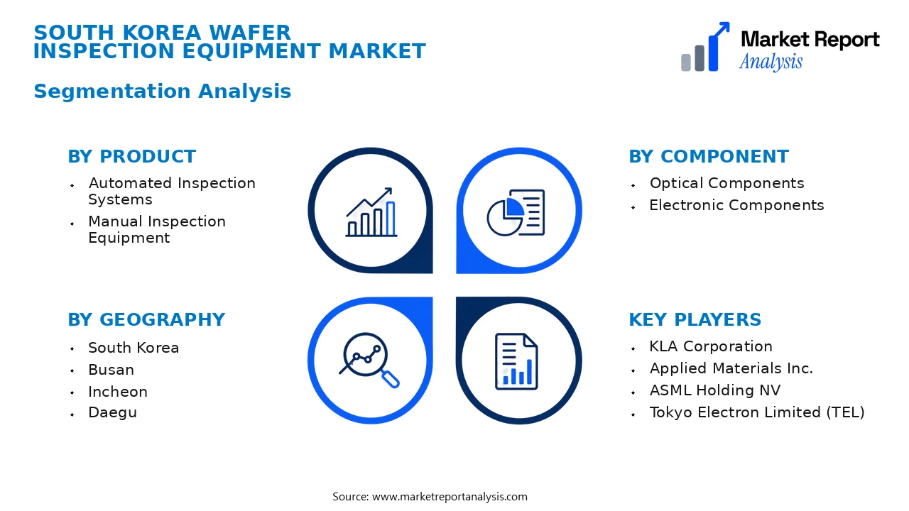
The South Korea Wafer Inspection Equipment Market is segmented into various categories including product type, component, application, industry vertical, and geographic location within South Korea. These segments reflect the diverse range of inspection needs across the semiconductor manufacturing landscape and highlight regional and technological nuances that influence market dynamics.
- Product
- Automated Inspection Systems: These systems utilize advanced automation technologies to perform high-throughput, precise wafer inspection, essential for meeting the growing demands of high-volume semiconductor fabrication facilities in South Korea.
- Manual Inspection Equipment: While less prevalent, manual inspection tools are still used for specialized or low-volume wafer inspections, serving niche applications and quality assurance processes in certain South Korean fabs.
- Component
- Optical Components: Optical inspection components, including high-resolution cameras and lasers, are crucial for defect detection on wafer surfaces, driving adoption in South Korea’s ultra-fine process nodes.
- Electronic Components: Including processing units and sensors, these components enhance defect analysis accuracy, emphasizing the need for integrated, intelligent inspection solutions tailored for complex wafer architectures.
- Application
- Defect Detection: The primary application focuses on identifying particles, scratches, and pattern anomalies that compromise chip performance, crucial in maintaining South Korea’s reputation for high-quality semiconductors.
- Thickness and Layer Measurement: Accurate measurement of wafer layer thicknesses and uniformity is vital for process control, especially in advanced nodes like 3nm and below, fueling demand for sophisticated inspection equipment.
- Industry Vertical
- Foundries: Major foundries in South Korea, such as Samsung and SK Hynix, are significant consumers of wafer inspection equipment due to their extensive production volumes and push towards miniaturization.
- IDM Companies: Integrated Device Manufacturers focus on in-house wafer inspection to ensure quality and optimize process parameters, leading to substantial market share within South Korea’s semiconductor sector.
- Geography
- South Korea: As the largest market, South Korea hosts multiple leading semiconductor manufacturers and research institutes, with major production hubs in Seoul, Busan, Incheon, Daegu, Daejeon, Gwangju, Ulsan, and Suwon.
- Seoul: The capital hosts regional HQs, R&D centers, and fabs, making it a central hub for wafer inspection equipment supply and technological innovation.
- Busan: Known for its thriving electronics manufacturing sector, Busan's industrial clusters demand advanced inspection tools for high-volume wafer production.
- Incheon: With proximity to Incheon International Airport and logistics infrastructure, Incheon is vital for import/export and distribution of wafer inspection equipment.
- Daegu: Emerging as a technology hub, Daegu emphasizes semiconductor research and development, rapidly increasing the adoption of next-generation inspection solutions.
- Daejeon: Home to government R&D labs and universities, Daejeon is pivotal for innovative inspection technologies and pilot projects in wafer manufacturing.
- Gwangju: As a regional industrial cluster, Gwangju supports local semiconductor startups and supply chain companies requiring tailored inspection apparatuses.
- Ulsan: Industrial powerhouse with large manufacturing facilities, Ulsan’s demand for wafer inspection equipment is driven by automotive and electronics segment growth.
- Suwon: Close to Seoul, Suwon’s electronics manufacturing ecosystem sustains a robust market for wafer inspection, especially for smaller production runs and specialized applications.
- South Korea: As the largest market, South Korea hosts multiple leading semiconductor manufacturers and research institutes, with major production hubs in Seoul, Busan, Incheon, Daegu, Daejeon, Gwangju, Ulsan, and Suwon.
Competitive Intelligence
The South Korea Wafer Inspection Equipment Market is highly competitive, characterized by significant market concentration among top-tier players such as KLA Corporation and AMETEK. These firms leverage advanced product innovation, integrating AI and machine learning to enhance defect detection accuracy, which serves as a key differentiator. Business strategies primarily focus on strengthening local R&D capabilities, establishing strategic partnerships with leading chip manufacturers, and expanding manufacturing footprints within Seoul and other tech hubs. Recent acquisitions have centered on consolidating technological expertise and broadening product portfolios, enabling firms to offer comprehensive inspection solutions. Expansion strategies in South Korea emphasize collaboration with domestic semiconductor firms and government-backed initiatives to support innovation, reflecting a proactive approach to capture market share. Companies invest heavily in R&D, particularly in developing high-resolution, automated inspection systems that meet stringent local standards. This competitive landscape fosters rapid technological advancements and differentiation, positioning South Korea as a global leader in wafer inspection innovation, with regional disparities in activity driven by proximity to semiconductor manufacturing clusters.
Leading Company Profiles
The South Korea wafer inspection equipment market is fiercely competitive, featuring several key players pushing technological boundaries through innovation, strategic alliances, and capacity expansions to meet rising demand for advanced semiconductor manufacturing solutions.
- KLA Corporation
- Applied Materials Inc.
- ASML Holding NV
- Tokyo Electron Limited (TEL)
- Hitachi High-Technologies Corporation
- NuFlare Technology, Inc.
- Veeco Instruments Inc.
- Advantest Corporation
- Lasertec Corporation
- Shimadzu Corporation
KLA Corporation
KLA specializes in process control and yield management solutions for the semiconductor and related industries, offering high-precision inspection tools crucial for advanced wafer processing in South Korea’s chip manufacturing hubs.
Applied Materials Inc.
As a global leader in materials engineering solutions, Applied Materials provides state-of-the-art inspection and metrology systems that enable leading South Korean fabs to enhance chip performance and manufacturing efficiency.
ASML Holding NV
Primarily known for its lithography equipment, ASML also develops wafer inspection solutions integrated with its photolithography systems, supporting South Korea’s pursuit of cutting-edge semiconductor technology.
Tokyo Electron Limited (TEL)
TEL focuses on semiconductor production equipment that includes advanced inspection systems, strengthening South Korea’s key role in the global semiconductor supply chain through innovation-backed capacity expansion.
Hitachi High-Technologies Corporation
Hitachi provides a comprehensive portfolio of inspection apparatus, including optical and electron microscopes tailored for wafer inspection, vital for quality control in South Korean semiconductor fabs.
NuFlare Technology, Inc.
Specialized in defect review and inspection tools, NuFlare’s solutions are increasingly adopted by South Korean foundries aiming for higher yields and defect detection accuracy at advanced process nodes.
Veeco Instruments Inc.
Veeco develops metrology and inspection systems mainly for memory and logic chips, facilitating process optimization and defect detection, key to South Korea’s thriving memory semiconductor industry.
Advantest Corporation
Advantest offers a broad range of semiconductor testing and inspection equipment, supporting South Korea's demands for high-throughput wafer inspection solutions for advanced fabrication lines.
Lasertec Corporation
Lasertec specializes in optical inspection systems employing laser technology, which are crucial for defect detection on wafers at increasingly finer semiconductor process nodes in South Korea.
Shimadzu Corporation
Shimadzu provides high-resolution inspection and metrology instruments tailored to meet the rigorous demands of South Korea’s semiconductor industry for quality and process control.
Strategic Business Developments
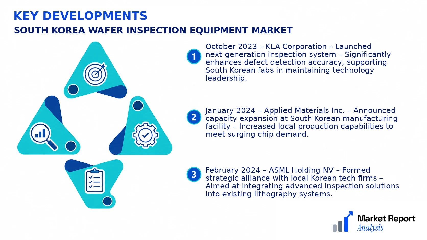
- October 2023 – KLA Corporation – Launched next-generation inspection system – Significantly enhances defect detection accuracy, supporting South Korean fabs in maintaining technology leadership.
- January 2024 – Applied Materials Inc. – Announced capacity expansion at South Korean manufacturing facility – Increased local production capabilities to meet surging chip demand.
- February 2024 – ASML Holding NV – Formed strategic alliance with local Korean tech firms – Aimed at integrating advanced inspection solutions into existing lithography systems.
- March 2024 – Tokyo Electron Limited – Invested in new R&D center in Seoul – Focused on developing innovative wafer inspection technologies tailored for South Korean industry needs.
- April 2024 – Hitachi High-Technologies – Acquired a local inspection services startup – Strengthening its service footprint and product integration in South Korea’s semiconductor sector.
Frequently Asked Questions
What is the South Korea Wafer Inspection Equipment Market?
The South Korea Wafer Inspection Equipment Market encompasses the manufacturing, sales, and deployment of equipment used to inspect semiconductor wafers for defects and inconsistencies. It is a crucial part of the semiconductor industry, supporting the production of high-quality chips for various applications.
What is the current market size of South Korea Wafer Inspection Equipment Market?
As of 2026, the South Korea Wafer Inspection Equipment Market is valued at approximately USD 2.3 Billion, reflecting the country’s robust semiconductor manufacturing infrastructure and technological advancements, which drive continual demand for sophisticated inspection solutions.
What factors are driving the South Korea Wafer Inspection Equipment Market?
Key drivers include increasing semiconductor production, technological innovations in inspection equipment, stringent quality standards, rising demand for miniaturization, and government incentives for domestic semiconductor R&D, all of which bolster demand for advanced wafer inspection tools in South Korea.
Which South Korean city leads the South Korea Wafer Inspection Equipment Market?
Seoul leads the market, given its status as the country’s semiconductor hub, home to major industry players, R&D centers, and technological universities, which collectively foster a highly innovative environment for wafer inspection equipment development.
Which segment is expected to grow the fastest?
The defect detection segment is anticipated to experience the fastest growth, driven by the increasing complexity of wafer designs and the need for ultra-precise inspection to minimize yield loss and improve overall chip quality.
Who are the leading companies operating in the South Korea Wafer Inspection Equipment Market?
Leading companies include Tokyo Electron, KLA Corporation, and Hermes Microvision, alongside local players like SAMSUNG Electronics and SK Hynix, collectively advancing the market with innovative inspection solutions tailored for South Korea’s semiconductor industry.
Analyst Perspective
The South Korea Wafer Inspection Equipment Market is poised for sustained growth, driven by ongoing advancements in semiconductor manufacturing and increasing demand for smaller, more complex chip architectures. Long-term prospects remain robust due to Korea’s strategic focus on leading-edge process nodes and continuous R&D investments in inspection technologies. Commercial opportunities are concentrated around high-precision inspection equipment suitable for advanced logic and memory chips, especially in regions like Seoul and surrounding metropolitan areas, which host major fabs and R&D centers. Technological evolution emphasizes AI-powered defect detection, automation, and inline inspection solutions, promising improved yield and reduced defect rates. Investment priorities should favor innovations in multi-layer inspection and zoom-in capabilities to meet evolving industry requirements. Competitive intensity is expected to remain high, with local firms enhancing their R&D efforts to maintain technological edge. Key city-level prospects in Seoul and the adjacent Gyeonggi Province offer substantial growth potential, supported by Korea’s active semiconductor ecosystem and government incentives for high-tech manufacturing, setting a strategic foundation for sustained leadership in wafer inspection technology.
