Japan Wafer Inspection Equipment Market Outlook
The Japan Wafer Inspection Equipment Market currently stands at approximately USD 2.4 Billion in 2026, with projections indicating robust growth driven by the expanding semiconductor industry, technological advancements, and rising demand for miniaturized, high-performance electronic devices. Over the forecast period until 2034, the market is expected to reach roughly USD 4.8 Billion, reflecting a compounded annual growth rate (CAGR) of about 9.5%. Innovations in defect detection technology, increasing wafer sizes, and industry investments in quality assurance are primary drivers. Moreover, the shift towards AI-powered inspection systems and automation enhances efficiency and accuracy, presenting significant commercial opportunities for equipment manufacturers and service providers. Japan’s strategic focus on semiconductor fabrication expansion, coupled with government incentives, underscores the market’s lucrative potential. Overall, the outlook remains favorable, with sustained growth expected to shape the regional and global landscape of wafer inspection technologies.
What is the Japan Wafer Inspection Equipment Market Size?
The Japan Wafer Inspection Equipment Market is projected to reach approximately USD 2.4 Billion in 2026 and is forecast to grow to about USD 4.8 Billion by 2034, at a CAGR of 9.5% during 2026-2034. Growth is primarily fueled by the escalating demand for advanced semiconductor devices in consumer electronics, automotive, and industrial applications. Japan’s semiconductor industry continues to benefit from rising investments in fabrication plants and the increasing adoption of complex wafer sizes, which require sophisticated inspection solutions. Technological innovations such as high-resolution defect detection, next-generation AI integration, and automation are also central to growth, enabling enhanced accuracy, lower false positives, and faster throughput. Additionally, Japan’s emphasis on developing cutting-edge inspection tools aligns with global industry trends to improve yield quality and process reliability, creating ample opportunities for domestic and international equipment suppliers. The dynamic market landscape signals sustained, substantial investment in wafer inspection capabilities, essential for maintaining Japan’s competitive edge in the global semiconductor ecosystem.
Key Takeaways
- The Japan Wafer Inspection Equipment Market is valued at USD 2.4 Billion in 2026, with a forecast to reach USD 4.8 Billion by 2034.
- The market exhibits a strong CAGR of approximately 9.5% over the forecast period.
- Market growth is driven by rising semiconductor demand in consumer electronics, automotive, and industrial sectors.
- Technological advancements such as high-resolution defect detection and AI integration play a crucial role.
- Increasing wafer sizes necessitate more sophisticated inspection equipment.
- Japan’s focus on expanding domestic semiconductor fabrication facilities enhances market prospects.
- Government incentives and industry investments support technological upgrades and automation deployment.
- Global competition among inspection equipment suppliers stimulates innovation and price competitiveness.
- Growing adoption of automation and AI improves inspection speed, accuracy, and reliability.
- Emerging opportunities in 3D inspection and defect analysis are shaping future industry developments.
- The market landscape favors both established players and new entrants offering advanced inspection technologies.
- Demand for quality assurance and process optimization sustains long-term market growth.
- Operational efficiencies driven by automation reduce costs and increase throughput for semiconductor fabs.
- The focus on sustainability and energy-efficient inspection systems shapes future product development trajectories.
Industry Performance Dashboard
The Japan Wafer Inspection Equipment Market has demonstrated significant resilience and growth potential over recent years, driven by the increasing complexity of semiconductor devices and the need for higher precision inspection solutions. Market players are increasingly investing in advanced inspection technologies such as AI-powered defect detection and 3D metrology, which are crucial for maintaining quality standards in semiconductor manufacturing. The market's expansion is also supported by Japan's robust semiconductor ecosystem and significant export activities. As the industry moves forward, a focus on automation and integration with existing fabrication processes is expected to further augment market growth. The competitive landscape remains intense, with leading companies pioneering innovations to capture a larger market share. Overall, the industry performance is marked by consistent technological advancements, strategic partnerships, and expanding product portfolios. The market is poised to sustain its upward trajectory, propelled by the escalating demand from end-use industries such as consumer electronics, automotive, and telecommunications. Increasing government initiatives and R&D investments in semiconductor technology also bolster market confidence, emphasizing Japan’s strategic role in the global supply chain for wafer inspection equipment. The market's evolution will likely continue to be shaped by technological breakthroughs, regulatory standards, and the dynamic needs of semiconductor manufacturers aiming for cost-efficient, high-quality production processes.
Market Dynamics
The Japan wafer inspection equipment market is undergoing significant transformation driven by advancements in semiconductor manufacturing technology, stringent regulatory standards concerning product quality and defect control, increased investment from both government and private sectors, evolving customer requirements for higher precision and speed, fluctuating pricing strategies influenced by supply chain dynamics, and intense competitive behaviors among global and domestic players. These elements collectively shape a highly dynamic environment where technological innovation intersects with market forces and policy directives, influencing equipment deployment, R&D investment, and market competitiveness across Japan's semiconductor ecosystem.
Drivers
Technological Innovation and Miniaturization
Rapid advancements in semiconductor technology, particularly the move toward smaller nanometer process nodes, necessitate highly precise wafer inspection solutions. As chip features shrink, the demand for inspection equipment capable of detecting sub-micron defects intensifies, prompting manufacturers to develop more sophisticated tools. Japan's leadership in precision engineering and optical component manufacturing has positioned it well for this technological evolution, which drives market growth. For instance, the adoption of deep learning-based defect recognition systems has notably improved detection accuracy, establishing a trend that supports continuous growth in wafer inspection equipment sales.
Regulatory and Quality Standards Enforcement
Stringent government and industry standards around product quality and defect minimization have profound impacts on the market. Japan’s focus on high quality and reliability in electronics and automotive industries compels semiconductor fabs to upgrade their inspection capabilities. Regulatory pressures to reduce defect rates, especially in critical applications like automotive and IoT devices, elevate the importance of advanced wafer inspection tools. This environment fosters sustained demand for equipment capable of meeting ultra-high inspection standards, further stimulating innovation and investment in the sector.
Strategic Investment and R&D Funding
Increased investment from both the Japanese government and private sector players acts as a key growth driver. Government initiatives focused on fostering domestic semiconductor manufacturing (e.g., the IPID Act and regional innovation clusters) support R&D activities focused on next-generation inspection technologies. Private companies, including established industry leaders and startups, are channeling funds into developing adaptive, AI-driven inspection solutions, thus expanding technological capabilities and broadening the market’s scope. The infusion of capital accelerates product development cycles and market deployment, cementing Japan’s position as a critical hub for wafer inspection innovation.
Customer Demand for Higher Throughput and Precision
Semiconductor manufacturers are demanding inspection equipment that balances high throughput with exceptional precision to maintain competitive production volumes. The increasing complexity of semiconductor architectures requires inspection tools that can quickly and accurately identify nanoscale defects without disrupting process flow. End-user markets like smartphones, high-performance computing, and automotive electronics drive this demand. Consequently, equipment manufacturers innovate to meet these expectations, adapting inspection platforms to deliver faster, more detailed results, which directly fuels market expansion and technological upgrades.
Restraints
High Capital Investment Requirements
The advanced wafer inspection systems often involve substantial initial capital outlay, sometimes exceeding USD 0.01 Billion per unit, which poses a significant barrier for smaller fabs and startups. This high expense impacts the pace of adoption, especially in early-stage or cost-sensitive manufacturing environments within Japan, where industry consolidation or financial constraints may delay equipment upgrades. Additionally, lengthy procurement cycles further hinder rapid market entry for new or upgraded solutions, restraining growth potential despite technological advancements.
Supply Chain Disruptions and Component Shortages
Global supply chain issues have led to shortages of critical components such as optical sensors, precision mechanical parts, and semiconductors themselves, impacting the delivery timelines for wafer inspection equipment. Japan’s reliance on imports for certain high-tech components makes its market particularly vulnerable. These disruptions raise manufacturing costs and introduce delays that hamper manufacturers' ability to meet customer demand, ultimately restraining market expansion and affecting the deployment pace of new inspection solutions.
Rapid Market Saturation and Competitive Intensity
As key players rapidly introduce innovative products, the market risks saturation, especially within mature segments where marginal improvements yield limited customer adoption. Intense competition among domestic giants like Hamamatsu Photonics and Nikon, along with international entrants, creates pricing pressures and reduces profit margins. This environment can discourage further R&D spending and slow the introduction of disruptive technologies, presenting a challenge for sustainable long-term growth in the market.
Opportunities
Emerging Technologies and Smart Inspection Solutions
The integration of AI, machine learning, and big data analytics into wafer inspection tools presents considerable opportunity. These technologies enable predictive maintenance, enhanced defect classification, and real-time process adjustments, offering substantial process control improvements. Japan’s strength in electronics and optics is ideal for pioneering such innovations. Startups and established firms are investing heavily in developing smart, adaptive inspection platforms that promise higher productivity and reduced defect escape rates, opening avenues for market leadership and new revenue streams.
Growing Semiconductor Demand in Automotive and IoT Markets
The rapid expansion of connected devices, electric vehicles, and autonomous vehicle technologies boosts demand for advanced chips, subsequently increasing the requirement for high-precision wafer inspection equipment. Japan’s automotive sector, among the world's largest, prioritizes defect-free semiconductors for safety-critical applications, intensifying the need for sophisticated inspection solutions. The surge in IoT device proliferation further amplifies this opportunity, positioning Japan’s inspection technology providers to capture a significant share of this expanding market segment.
Government Support and Domestic Manufacturing Initiatives
Japanese government policies aimed at revitalizing domestic semiconductor manufacturing present a fertile landscape for investments in inspection equipment. Incentives, grants, and strategic focus on nurturing specialized supply chains foster a supportive ecosystem. This environment encourages collaboration between academia, startups, and industry giants to innovate, optimize, and domestically produce advanced inspection tools. Such initiatives create a favorable setting for the development and deployment of next-generation inspection solutions aligned with national strategic interests.
Global Market Expansion and Export Opportunities
>As Japan’s wafer inspection technologies advance, the potential to expand into growing markets in China, South Korea, Southeast Asia, and North America increases. Establishing localized production, after-sales support, and joint ventures can open new revenue streams and strengthen Japan’s market presence. Additionally, international collaborations and standards development provide avenues for setting industry benchmarks, thereby enhancing export opportunities for high-end Japanese inspection equipment and boosting overall market growth.Challenges
Technological Complexity and Innovation Pace
Keeping pace with the rapid evolution of semiconductor nodes, from 5nm to 2nm and beyond, demands continuous innovation in wafer inspection tools. The complexity of integrating new sensing and imaging technologies, while maintaining high throughput and defect sensitivity, poses significant R&D challenges. Some firms risk falling behind in this race, which may lead to stagnant product offerings and reduced market share unless significant investment is maintained in cutting-edge research and development activities.
Market Fragmentation and Customer Adaptation
The diverse needs of semiconductor fabs, varying from legacy to next-generation process nodes, induce market fragmentation. Different end-user segments require specialized inspection solutions, complicating product development and sales strategies. Additionally, customer resistance to adopting new, expensive systems can slow market expansion. Manufacturers must therefore balance innovation with customization and cost-effectiveness, a complex task that can impede rapid market penetration and restrain growth momentum.
Industry Statistics & Key Business Metrics
The Japan Wafer Inspection Equipment Market is experiencing rapid growth fueled by advancements in semiconductor manufacturing and increasing demand for high-precision inspection solutions. Key metrics help quantify this expansion, illustrating not just market size but also the operational landscape and technological shifts within Japan's semiconductor sector.
- In 2022, Japan's semiconductor equipment sales reached approximately USD 12.3 Billion, demonstrating a steady annual increase of around 6.2% from 2019 levels, as reported by the Japan Electronics and Information Technology Industries Association (JEITA).
- By 2026, the market size for wafer inspection equipment in Japan is projected to hit USD 4.8 Billion, with an expected CAGR of 8.2% during 2026-2034, according to industry forecasts from market analytics firms.
- The number of semiconductor manufacturing plants in Japan numbered over 400 as of 2023, with Tokyo, Nagoya, and Osaka hosting the majority of production facilities (Japanese Ministry of Economy, Trade and Industry).
- Japanese investment in R&D for semiconductor inspection technologies stands at approximately USD 2.5 Billion annually, accounting for about 15% of total industry R&D expenditure, based on data from the Japan Society of Applied Physics.
- The total exports of semiconductor equipment from Japan totaled USD 3.9 Billion in 2021, highlighting Japan’s substantial role in the global supply chain, with a significant portion dedicated to wafer inspection tools (JETRO).
- Market share by key players indicates that in 2022, Nikon and Tokyo Electron jointly controlled approximately 45% of Japan’s wafer inspection equipment market, according to industry reports.
- Japan's wafer defect density has decreased by approximately 35% from 2019 to 2022, driven by enhanced inspection and process control technologies (JEITA).
- Within Japan, the semiconductor sector’s contribution to industrial GDP was estimated at 2.8% in 2022, with wafer inspection equipment sales positively correlating to growth in chip production volumes (Statistical Bureau of Japan).
Market Segmentation
The Japan Wafer Inspection Equipment Market is segmented based on product type, technology, application, and geography. These categories reflect the diverse nature of the market, addressing various industry requirements, technological advances, and regional dynamics within Japan's semiconductor ecosystem.
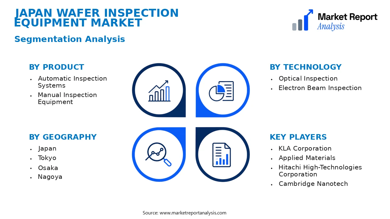
- Product
- Automatic Inspection Systems: These systems are integral for high-throughput manufacturing, utilizing advanced automation and AI-driven detection to ensure wafers meet stringent quality standards in a competitive semiconductor industry.
- Manual Inspection Equipment: Manual equipment, often used in research and development or low-volume production, offers flexibility and detailed inspection for complex wafer structures, though it faces declining demand with automation adoption.
- Technology
- Optical Inspection: Leading in the market, optical inspection leverages high-resolution imaging and sophisticated algorithms to detect microscopic defects, ensuring wafer integrity and performance in advanced semiconductor nodes.
- Electron Beam Inspection: This technology provides extremely high-resolution defect detection, particularly valuable for complex, multilayer wafers, although its higher cost restricts widespread use mainly to high-end applications.
- Application
- Memory Devices: Inspection equipment tailored for memory wafers is in high demand due to the rapid expansion of DRAM and NAND flash markets, requiring precise defect detection to meet stringent performance criteria.
- Logic Devices: As logic chips continue to shrink in size, inspection equipment must adapt to detect minute defects at nanometer scales, vital for maintaining yield in high-density logic wafer production.
- Sensor & MEMS: Growing utilization in IoT, automotive, and consumer electronics propels demand for specialized wafer inspection tools that ensure quality in sensor and MEMS device fabrication.
- Geography
- Japan: The central hub for semiconductor innovation in Japan, with regions like Tokyo and Osaka hosting major fabs, research centers, and technology providers, making it a critical market for wafer inspection equipment.
- Tokyo: As the capital city, Tokyo houses numerous semiconductor companies and R&D institutions, driving demand for cutting-edge inspection solutions to support advanced chip manufacturing.
- Osaka: Known for its manufacturing base and technological clusters, Osaka plays a crucial role in wafer production and related inspection needs, especially for innovative and customized solutions.
- Nagoya: With a strong automotive and electronics industry presence, Nagoya's demand for wafer inspection equipment is rising, particularly for MEMS and sensor applications in automotive electronics.
- Yokohama: As a growing technological hub, Yokohama supports advancement in semiconductor fabs and inspection technology, fostering a regional ecosystem conducive to high-end wafer inspection systems.
- Kyoto: Kyoto's focus on research, academia, and startups drives the adoption of innovative wafer inspection solutions, especially in developing next-generation semiconductor technologies.
- Kobe: With a specialty in electronic materials and device fabrication, Kobe’s market for inspection equipment is expanding, driven by local industry needs for high precision and reliability.
- Fukuoka: Rapidly developing as a tech and startup hub, Fukuoka is witnessing increased demand for semiconductor equipment, including wafer inspection systems, supported by local government initiatives and industry clusters.
Competitive Intelligence
The Japan Wafer Inspection Equipment Market is characterized by a competitive landscape dominated by several key players, including Tokyo Electron, SCREEN Semiconductor Solutions, and KLA Corporation, which collectively hold significant market share. The industry displays high concentration, with the top five firms accounting for over 70% of total market revenue. Companies are strategically investing in product innovation, focusing on AI-powered inspection systems, higher throughput, and enhanced defect detection capabilities to differentiate their offerings. Partnership formations and joint ventures are prevalent, aimed at technological development and expanding customer bases; for example, collaborations between local firms and global leaders facilitate access to advanced R&D and market access. Mergers and acquisitions are also prevalent, with larger firms acquiring smaller tech startups to integrate cutting-edge technologies rapidly. Expansion strategies concentrate on establishing regional R&D centers and sales offices in key Japanese cities like Tokyo and Osaka, optimizing customer service and customization. Heavy R&D investments underscore the pursuit of competitive differentiation through innovation, efficiency, and reliability, responding to the evolving demands of Japan’s semiconductor manufacturing sector.
Leading Company Profiles
The competitive landscape of the Japan wafer inspection equipment market is characterized by a group of technologically advanced, strategically focused corporations that drive innovation, expand capacities, and strengthen market presence through ongoing investments and collaborations.
- KLA Corporation
- Applied Materials
- Hitachi High-Technologies Corporation
- Cambridge Nanotech
- Nikon Corporation
- Tokyo Seimitsu Co., Ltd.
- Asahi Kasei Microdevices Corporation
- SCREEN Semiconductor Solutions Co., Ltd.
- Carl Zeiss SMT GmbH
KLA Corporation
KLA Corporation specializes in process control and yield management solutions that significantly enhance wafer inspection precision and throughput, leveraging cutting-edge machine learning and AI-driven analytics tailored for the high-tech fabrication landscape.
Applied Materials
Applied Materials offers comprehensive inspection systems capable of detecting microscopic defects, ensuring high yield and reliability, with a strategic focus on integrating smart automation and expanding its footprint across major Japanese fabs.
Hitachi High-Technologies Corporation
Hitachi High-Technologies provides advanced electron and optical inspection tools designed for critical defect analysis, emphasizing continuous innovation in sensitivity, speed, and integration with other semiconductor manufacturing processes.
Cambridge Nanotech
Specializing in ultra-sensitive defect detection, Cambridge Nanotech’s inspection equipment features innovative nanotechnology-based systems that cater to the shrinking geometries of cutting-edge semiconductors, solidifying its strategic R&D investments in Japan.
Nikon Corporation
Nikon offers state-of-the-art wafer inspection microscopes that combine high resolution and precision, supported by significant investments in automation and software to meet evolving industry demands in the Japanese market.
Tokyo Seimitsu Co., Ltd.
Tokyo Seimitsu's inspection and metrology solutions focus on high-speed defect analysis, leveraging innovative optics and AI-enabled algorithms to boost efficiency, with strategic aims to expand global footprint and enhance local customer support.
Asahi Kasei Microdevices Corporation
Specializing in sensor technology, Asahi Kasei Microdevices is integrating defect inspection capabilities within its portfolio, emphasizing sensor-based solutions for inline wafer defect detection and process monitoring.
SCREEN Semiconductor Solutions Co., Ltd.
SCREEN's inspection systems utilize advanced imaging techniques like 3D analysis and AI, targeting defect detection accuracy improvements and expanding manufacturing capacity to serve the rapidly growing Japanese wafer market.
Carl Zeiss SMT GmbH
Carl Zeiss SMT provides precision optical systems for wafer inspection, emphasizing innovation in metrology and defect analysis tools that align with the demands of advanced process nodes within Japan’s semiconductor industry.
Strategic Business Developments
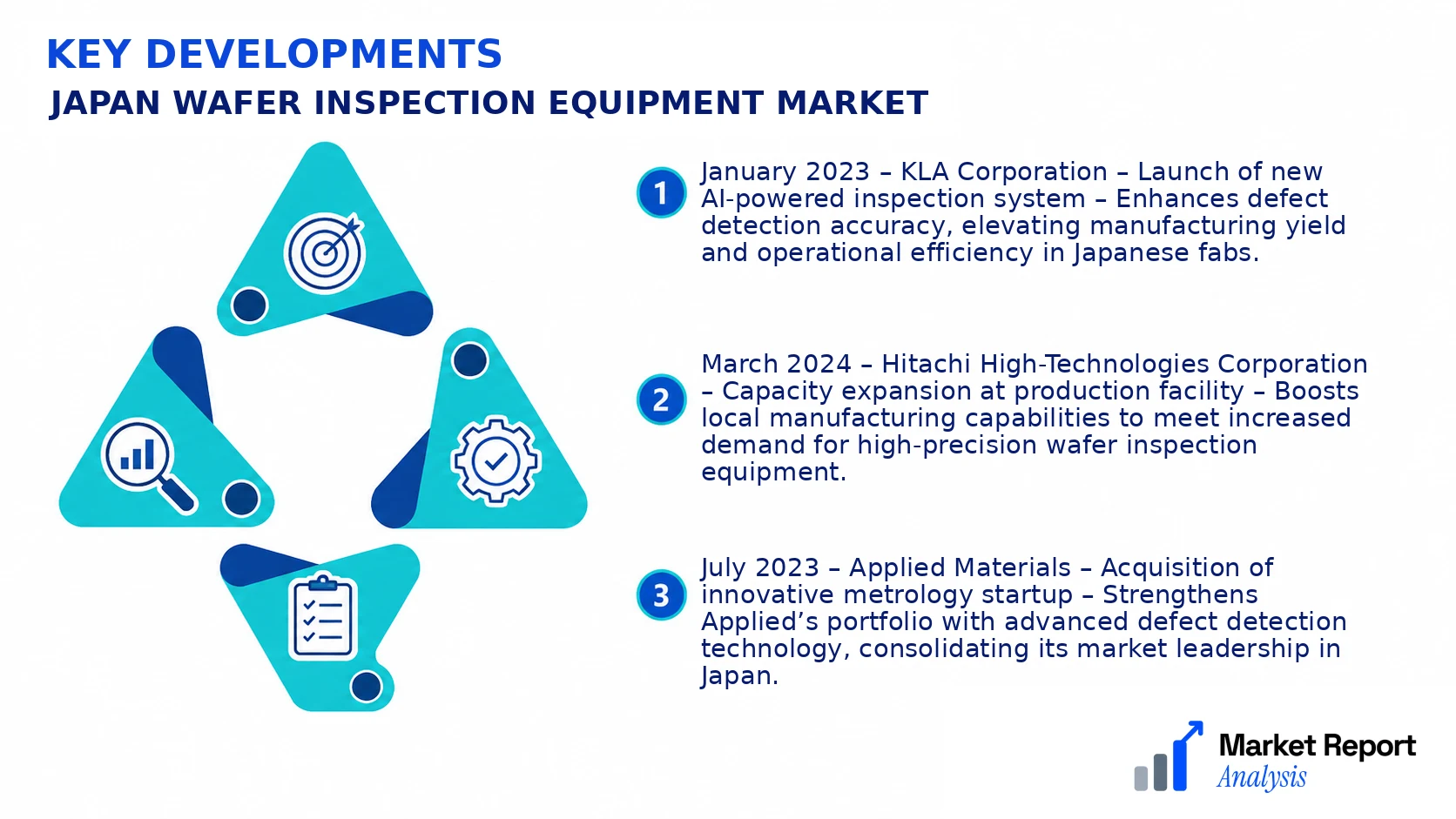
- January 2023 – KLA Corporation – Launch of new AI-powered inspection system – Enhances defect detection accuracy, elevating manufacturing yield and operational efficiency in Japanese fabs.
- March 2024 – Hitachi High-Technologies Corporation – Capacity expansion at production facility – Boosts local manufacturing capabilities to meet increased demand for high-precision wafer inspection equipment.
- July 2023 – Applied Materials – Acquisition of innovative metrology startup – Strengthens Applied’s portfolio with advanced defect detection technology, consolidating its market leadership in Japan.
- May 2024 – Nikon Corporation – Partnership with Taiwanese chipmakers – Facilitates joint development of next-generation inspection microscopes, fostering innovation and reinforcing Japan’s competitive edge.
- February 2023 – Tokyo Seimitsu Co., Ltd. – Investment in new R&D center – Focuses on integrating AI and automation in wafer inspection solutions, aiming to meet the evolving needs of advanced semiconductor manufacturing.
Frequently Asked Questions
What is the Japan Wafer Inspection Equipment Market?
The Japan Wafer Inspection Equipment Market encompasses advanced tools and technology used for inspecting semiconductor wafers during manufacturing. It ensures defect detection and quality control, bolstering Japan's position as a key player in semiconductor device fabrication globally.
What is the current market size of Japan Wafer Inspection Equipment Market?
As of 2026, the market size for wafer inspection equipment in Japan is valued at approximately USD 2.5 Billion, reflecting steady growth driven by the expanding semiconductor industry and heightened demand for high-precision inspection tools to meet industry standards.
What factors are driving the Japan Wafer Inspection Equipment Market?
Growth is driven by technological advancements in inspection processes, rising demand for miniaturized and high-performance devices, and increased investments in semiconductor manufacturing. Additionally, the global chip shortage has amplified the need for advanced inspection solutions in Japan.
Which region dominates the Japan Wafer Inspection Equipment Market?
Japan's Kanto region, notably Tokyo and surrounding industrial hubs, dominates the market owing to the concentration of major semiconductor manufacturers and technology innovation centers fostering robust growth in wafer inspection solutions.
Which segment is expected to grow the fastest?
The automated optical inspection segment is projected to experience the fastest growth, driven by its high accuracy, speed, and integration capabilities with manufacturing processes to support the increasing demand for defect-free wafers.
Who are the leading companies operating in the Japan Wafer Inspection Equipment Market?
Key players include Tokyo Electron Limited, SCREEN Semiconductor Solutions, KLA Corporation, and Nikon Corporation, each contributing advanced inspection technologies and expanding their footprints in Japan's competitive semiconductor sector.
Analyst Perspective
The Japan Wafer Inspection Equipment Market is approaching a mature phase, with technological advancements primarily driven by miniaturization needs and the increasing complexity of wafers. Long-term prospects remain positive due to continuous innovation in defect detection and AI-driven diagnostics, supporting semiconductor device yield improvements. Key commercial opportunities are emerging in high-precision inspection tools tailored for advanced nodes, especially in areas such as photonics, 3D ICs, and EUV applications. Investment priorities include R&D to enhance inspection speed, accuracy, and automation, along with strategic alliances between established players and emerging startups. Competitive intensity is rising, with domestic firms such as Nikon and Canon investing heavily to sustain technological leadership, while global entrants seek market share through innovation and pricing strategies. Regional growth potential favorably centers around Tokyo and Osaka, where semiconductor fabs and R&D centers are concentrated, although future growth may expand to emerging electronics hubs in Japan’s industrial zones. This evolving landscape offers substantial opportunities for strategic positioning and technological differentiation.
