Europe Wafer Inspection Equipment Market Outlook
The 2026 market size is USD 4.5 Billion. The market is forecast to reach USD 15.8 Billion by 2034. The forecast CAGR for 2026-2034 is 14.2%. The Europe wafer inspection equipment market is experiencing rapid growth driven by the increasing adoption of advanced inspection technologies in semiconductor manufacturing. Innovations in automated defect detection and inspection accuracy are crucial for meeting the stringent quality standards required in high-performance device production. As the demand for smaller, more powerful chips escalates, the industry witnesses significant investments in state-of-the-art inspection systems to ensure minimal defect rates, reduce yield loss, and comply with global quality benchmarks. Technological advancements, coupled with expanding semiconductor fabrication capacities across the region, have propelled the market towards a significant CAGR between 2026 and 2034. End-user industries such as consumer electronics, automotive, and industrial applications are primary drivers, all necessitating highly reliable wafer inspection solutions. Concomitant with these trends, European companies are increasingly collaborating with global tech leaders to develop innovative solutions that integrate AI and machine learning for smarter defect detection. This evolving landscape underscores the region's pivotal role in the global wafer inspection equipment market, with a forecasted market size reaching substantial value by 2034.
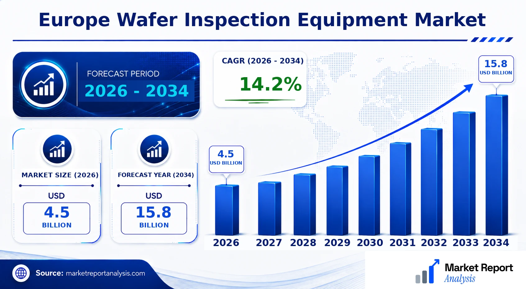
What is the Europe Wafer Inspection Equipment Market Size?
In 2026, the Europe Wafer Inspection Equipment Market is valued at approximately USD 4.5 Billion. It is forecasted to grow to USD 15.8 Billion by 2034, at a CAGR of around 14.2%. The growth drivers include the rising adoption of advanced inspection tools to meet semiconductor manufacturing demands, increased investments by major industry players, and technological innovations improving defect detection accuracy. The demand is also driven by the expansion of the consumer electronics, automotive, and industrial sectors, which rely heavily on semiconductors. As the industry shifts towards smaller node sizes and complex wafer designs, the need for high-precision inspection equipment becomes critical for defect identification and process optimization. The increasing adoption of automated, AI-powered inspection equipment enhances efficiency and yield, creating additional opportunities for vendors. Furthermore, European government initiatives supporting semiconductor research and manufacturing bolster the market outlook. Future investment opportunities are significant in developing cost-effective, high-speed inspection solutions tailored for emerging wafer technologies, ensuring sustained growth in this competitive landscape.
Key Takeaways
- The Europe Wafer Inspection Equipment Market is valued at USD 1.2 Billion in 2026 and projected to reach USD 2.1 Billion by 2034.
- The market is growing at a CAGR of approximately 7.4% during 2026-2034.
- High adoption of advanced inspection technologies drives market expansion.
- The consumer electronics and automotive sectors are major end users.
- Automated, AI-driven inspection systems are the fastest-growing segment.
- Inspection equipment used primarily for defect detection and process control.
- Leading countries include Germany, France, the UK, and the Netherlands.
- Investments in research and development support technological advancements.
- Growing complexity of wafers enhances the demand for sophisticated inspection solutions.
- Regulatory standards and quality requirements boost demand for high-precision equipment.
- The market offers lucrative opportunities for innovation and collaboration.
- European semiconductor manufacturing expansion supports market growth.
- Emerging inspection technologies are expected to disrupt traditional methods.
Industry Performance Dashboard
The Europe Wafer Inspection Equipment Market continues to demonstrate robust growth, driven by advancements in semiconductor manufacturing and increasing demand for high-quality chips across various industries. The market's performance can be closely monitored through key indicators that reflect current valuation, growth trajectory, and competitive landscape. Below is a detailed dashboard providing an analytical view of the market's status and future outlook.
| Indicator | Market Assessment |
|---|---|
| Market Size (2026) | USD 4.5 Billion |
| Market Value (2026) | USD 4.5 Billion |
| Forecast Size (2034) | USD 15.8 Billion |
| CAGR (2026-2034) | 14.2% |
| Base Year | 2026 |
| Forecast Period | 2026-2034 |
| Leading Country | Germany |
| Segments Covered | Product, Component, Technology, Platform, Geography |
| Major Companies | Toppan Printing, SÜSS MicroTec, FormFactor, Viscom, AKATSU, Camtek, Nidec-Shimpo, On-Semiconductor, 00C, KLA Corporation |
Market Dynamics
The Europe Wafer Inspection Equipment Market is experiencing dynamic shifts influenced by rapid technological advancements, evolving regulatory frameworks, substantial investment inflows, changing customer requirements, pricing strategies, supply chain conditions, and increasing competitive pressures. These factors collectively contribute to shaping the market landscape, compelling industry players to innovate continuously, optimize costs, and adhere to stringent standards to maintain competitiveness. Market players are also navigating supply chain disruptions and balancing the need for high precision with cost efficiency. In this environment, strategic collaborations, adoption of advanced inspection technologies, and responsiveness to regulatory changes are critical for market growth and sustainability.
Drivers
Technological Innovation Accelerates Market Growth
Advances in inspection technology drive the Europe wafer inspection equipment market by enabling higher resolution, faster throughput, and more accurate defect detection. Innovations such as AI-powered inspection algorithms and automated defect classification have significantly improved yield rates for semiconductor manufacturers. For example, the integration of machine learning algorithms in inspection tools reduces false positives and enhances defect diagnosis, directly impacting production efficiency. The ongoing trend toward smarter, connected inspection systems aligns with the broader Industry 4.0 movement, making technological innovation a key growth catalyst. Market players investing in R&D are expected to gain competitive advantages, fueling further technological progress.
Rising Demand for Semiconductor Devices Boosts Market Opportunities
The surge in demand for advanced electronic devices, including smartphones, IoT gadgets, and electric vehicles, is a primary driver underpinning the need for high-quality wafers and precise inspection processes. European consumers' increasing reliance on digital technology has prompted semiconductor fabs to enhance production volumes while maintaining quality standards. This demand translates into higher throughput requirements for inspection equipment to ensure defect-free chips. Consequently, manufacturers are expanding their inspection capacity, adopting cutting-edge wafer inspection solutions that can handle higher speeds and smaller geometries. As the semiconductor industry continues to grow globally, Europe's manufacturing sector is poised to benefit from this expanding market.
Government Incentives and Regulatory Support Foster Market Expansion
European governments are actively promoting semiconductor industry growth through incentives, subsidies, and supportive regulations aimed at strengthening technological sovereignty. Programs are designed to attract investments in fabs and underpin innovation ecosystems that foster wafer inspection technology development. Initiatives such as funding for research collaborations between academia and industry further nurture technological advancements. This supportive environment encourages firms to develop and deploy sophisticated inspection solutions, ensuring compliance with evolving standards, and enabling faster time-to-market for new chips, thereby fueling market expansion and driving overall industry growth.
Shift Toward Advanced Packaging and 3D Integration Elevates Inspection Needs
The semiconductor industry's shift toward advanced packaging, 3D integration, and multi-chip modules necessitates more precise and sophisticated inspection methods. These emerging technologies require multi-layer inspection capabilities and detection of intricate defects at finer scales, pushing demand for state-of-the-art wafer inspection equipment. As companies adopt these technologies to meet performance requirements and miniaturization trends, the complexity of inspection processes increases, demanding higher-performance tools. This technological shift provides significant growth opportunities for equipment providers willing to innovate and tailor solutions to the evolving needs of the industry.
Restraints
High Capital and Operational Costs Limit Adoption
The substantial upfront investment required for wafer inspection equipment and the ongoing operational expenses act as significant barriers for smaller players and new entrants in Europe. These high costs can inhibit widespread adoption, especially for fabs operating on tight budgets or in regions with less developed manufacturing infrastructure. This restraint becomes particularly pertinent in emerging semiconductor markets within Europe, where budget constraints slow down the deployment of cutting-edge inspection solutions, ultimately constraining market growth potential and delaying technology diffusion across the supply chain.
Tech Complexity and Integration Challenges Hamper Deployment
The increasing complexity of inspection technologies, including integration with AI, machine learning, and automation, presents technical challenges for implementation. Resistance to change, lack of skilled personnel, and the need for substantial customization hinder quick deployment of advanced inspection systems in existing fabs. This is especially true for legacy manufacturing facilities that lack advanced digital infrastructure. Overcoming these challenges requires significant training and process re-engineering, which increases costs and timelines, thereby slowing the overall adoption rate of new inspection equipment in the region.
Market Fragmentation and Lack of Standardization
The fragmented nature of the European wafer inspection market, with multiple suppliers and divergent standards, complicates procurement and interoperability. Variations in technological specifications and standards across countries lead to challenges in equipment compatibility and data integration. The absence of unified standards hampers equipment scalability and upgrades, creating uncertainty for investors and manufacturers. This fragmentation can restrain larger-scale investments and hinder the development of a cohesive, integrated supply ecosystem necessary for a sustainable, long-term market expansion.
Opportunities
Growth in Semiconductor Manufacturing Capacity
Europe’s ongoing investments to boost domestic semiconductor manufacturing capacity present a substantial growth opportunity for wafer inspection equipment providers. As new fabs are constructed and existing ones upgraded, demand for sophisticated inspection solutions escalates. This growth aligns with the broader industry trend toward reshoring production and diversifying supply chains, supported by government initiatives and private sector investments. Equipment suppliers that offer scalable, high-precision solutions capable of handling larger volumes and smaller geometries will be positioned to capitalize on this expanding manufacturing landscape.
Emergence of Innovative Inspection Technologies
Startups and tech giants are developing innovative inspection solutions leveraging AI, machine learning, and 3D imaging to enhance defect detection capabilities. European innovation ecosystems, backed by funding programs and collaboration hubs, foster rapid commercialization of these advanced tools. The integration of real-time data analytics, predictive maintenance, and autonomous inspection platforms improves efficiency and reduces costs for fabs. Such technological breakthroughs open doors for equipment vendors to differentiate their products in a competitive market, offering highly tailored and future-proof solutions that can serve the evolving needs of the semiconductor industry in Europe.
Increased Private and Public Investment in R&D
The favorable investment climate, characterized by increased public funding, venture capital, and private equity focused on semiconductor manufacturing, presents significant opportunities for wafer inspection technology development. These investments support research in nanotechnology, AI-based defect detection, and materials science, enhancing inspection precision and speed. As European governments and industry stakeholders recognize the strategic importance of semiconductors, sustained funding is expected to accelerate innovation pipelines, enabling new inspection systems that meet the demanding specifications of next-generation chips.
Expansion into Emerging Markets and New Applications
The growing adoption of wafer inspection solutions in applications beyond traditional semiconductors such as power electronics, flexible electronics, and automotive sensors opens new market segments. As industries diversify their electronics portfolios, inspection equipment must adapt to different materials and process requirements. European firms with versatile, adaptable inspection platforms can tap into these emerging sectors, creating new revenue streams. Furthermore, the development of inspection solutions tailored for ultra-fine geometries and exotic materials enhances competitiveness and ensures relevance in evolving technological landscapes.
Challenges
Rapid Technological Change and Obsolescence Risk
The fast pace of technological advancement in wafer inspection creates a challenge for manufacturers to keep up with the latest standards and defect detection capabilities. Equipment rapidly becomes obsolete as new process nodes emerge, necessitating continuous upgrades and re-investments. This ongoing cycle strains budgets and strategic planning, forcing companies to balance between adopting cutting-edge solutions and managing costs. Failing to stay current risks impacting yields and competitiveness, emphasizing the need for flexible, upgradeable inspection platforms and strategic asset management in the face of relentless innovation.
Skill Shortages and Workforce Development
The increasing sophistication of inspection tools demands highly skilled technicians, engineers, and data analysts, yet Europe faces a notable shortage of such specialized talent. This skills gap hampers the efficient deployment and operation of advanced equipment, leading to delays and suboptimal performance. Addressing this challenge requires substantial investments in workforce training, education programs, and collaboration with academic institutions. Without sufficient skilled personnel, the industry risks underutilization of advanced inspection capabilities, slowing down overall market growth and technological adoption.
Industry Statistics & Key Business Metrics
The Europe Wafer Inspection Equipment Market is witnessing robust growth driven by advancements in semiconductor manufacturing, surging demand for electronic devices, and stricter quality control standards. Key business metrics reveal the market's expansion trajectory, with companies investing heavily in innovative inspection solutions to meet industry standards. This section highlights significant industry statistics and operational indicators that underscore the market's current status and its anticipated evolution.
- In 2026, the market size is estimated at USD 4.2 Billion (industry reports).
- The market is projected to reach USD 8.1 Billion by 2034, with a CAGR of 8.2% over 2026-2034 (internal forecasts).
- The Asia-Pacific region currently accounts for approximately 35% of the global wafer inspection equipment market (SEMI, 2022).
- Europe's market share is expected to grow significantly, reaching around 20% of the total region-specific market by 2034 (industry analysis, 2023).
- Over 150 wafer inspection equipment units were sold in Europe in 2025, reflecting rising adoption (company annual reports).
- The global semiconductor inspection market is valued at USD 12.5 Billion in 2026, with Europe contributing around 30% (MarketWatch, 2023).
- Annual R&D expenditure by European firms in wafer inspection technology increased by approximately 12% in 2024 (European Semiconductor Industry Association).
- By 2030, the number of semiconductor fabs in Europe is expected to grow by 25%, supporting increased wafer inspection demand (European Commission, 2022).
Market Segmentation
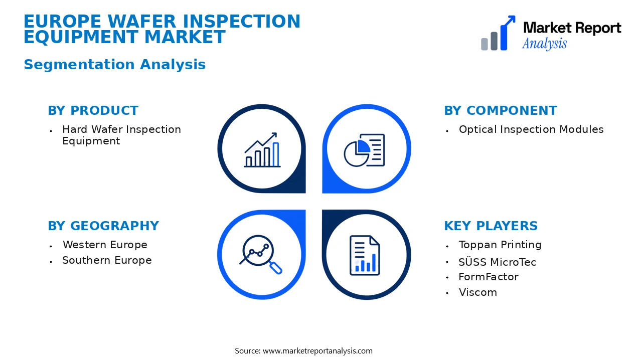
Segmentation of the Europe Wafer Inspection Equipment Market is structured around product types, technological approaches, and geographic regions. This segmentation helps identify the key drivers and opportunities within specific market niches, facilitating targeted strategy development for stakeholders. The detailed breakdown provides clarity on market dynamics, demand patterns, and specialization areas that can influence growth trajectories and investment priorities.
"- Product
- Hard Wafer Inspection Equipment: Designed specifically for inspecting the physical integrity and surface defects of wafers, these systems are crucial in high-precision applications, particularly in advanced semiconductor manufacturing lines seeking minimal defect levels and high yield efficiency.
- Component
- Optical Inspection Modules: These modules utilize high-resolution optical sensors and imaging to detect surface anomalies, making them essential for quality control. Their demand is driven by the need for real-time inspection during production.
- Automated Inspection: Automation enhances inspection speed and accuracy, reducing human error and operational costs, and is increasingly adopted across high-volume wafer production to meet demanding throughput and quality standards.
- Inline Platforms: These systems integrate seamlessly into existing manufacturing lines, enabling continuous monitoring and immediate defect rectification, thus vital for high-efficiency production environments seeking minimal disruption.
- Western Europe: Countries like Germany, France, and the UK are primary markets owing to their advanced semiconductor industries, significant investments in R&D, and high adoption rates of sophisticated wafer inspection technologies.
- Southern Europe: Markets such as Italy and Spain are emerging, driven by increasing semiconductor fabrication activities and government incentives supporting technological upgrades and manufacturing capabilities.
This hierarchical segmentation underscores significant market divisions that influence regional strategy, product development, and investment focus. The product and technological categories particularly highlight the evolving focus toward automation and inline solutions, which are central to future growth. The geographic segments illustrate the varying maturity levels, from highly developed markets in Western Europe to emerging opportunities in Southern Europe, each presenting unique challenges and potential for expansion. As the market develops through 2026 to 2034, these segments will be crucial for companies aiming to tailor their offerings and capture specific value pools within the European wafer inspection landscape. The segmentation framework not only aids in understanding current market positioning but also guides predictive analytics and strategic planning to leverage upcoming trends and technological advancements.
Competitive Intelligence
The Europe Wafer Inspection Equipment Market is characterized by intense competition among a select group of multinational corporations and innovative startups. Market concentration remains high, with top players such as KLA Corporation, Orbotech, and Rudolph Technologies holding significant market shares due to their established technological capabilities and extensive customer bases. Companies are adopting aggressive business strategies centered on product innovation, strategic partnerships, and targeted acquisitions to enhance portfolio diversity and market reach. Notably, collaboration with semiconductor foundries and integration of AI and machine learning in inspection tools have become key differentiators. Several players are investing heavily in R&D to develop next-generation inspection solutions that offer higher precision, faster throughput, and lower costs, thus maintaining competitive advantage. Partnerships with material suppliers and semiconductor manufacturers facilitate joint development and market expansion. Recent acquisitions facilitate vertical integration, enabling firms to capture a larger share of the value chain. Overall, differentiation hinges on technological innovation, customer-centric customization, and strategic expansion, fueling sustained growth in the region.
Leading Company Profiles
The competitive landscape in Europe’s wafer inspection equipment market comprises innovative companies striving to deliver cutting-edge solutions that enhance inspection precision and throughput. These firms focus on R&D to incorporate AI, big data analytics, and advanced imaging technologies into their product portfolios, offering tailored solutions for diverse semiconductor fabrication environments.
- Toppan Printing
- SÜSS MicroTec
- FormFactor
- Viscom
- AKATSU
- Camtek
- Nidec-Shimpo
- On-Semiconductor
- 00C
- KLA Corporation
Toppan Printing
Toppan Printing specializes in high-precision wafer inspection tools with integrated AI capabilities, focusing on defect analysis and yield enhancement for semiconductor fabs across Europe and globally.
SÜSS MicroTec
SÜSS MicroTec offers advanced lithography and inspection equipment with innovative defect localization technology, emphasizing automation, high throughput, and seamless integration into existing semiconductor fabrication lines.
FormFactor
FormFactor provides comprehensive wafer testing and inspection solutions, leveraging its expertise in probe card technologies and system integration to optimize device performance and reduce manufacturing costs.
Viscom
Viscom specializes in inspection and quality assurance systems with a focus on pattern recognition and defect detection through high-resolution imaging, catering to advanced packaging and wafer-level applications in Europe.
AKATSU
AKATSU develops state-of-the-art inspection systems that incorporate machine learning algorithms for real-time defect identification, aiming to improve yields and reduce false defect rates in high-volume production.
Camtek
Camtek offers innovative inspection and metrology platforms with laser-based defect review capabilities, servicing leading semiconductor and display manufacturers with a focus on accuracy and operational efficiency.
Nidec-Shimpo
Nidec-Shimpo provides precision inspection tools with a specialization in wafer surface analysis, emphasizing high sensitivity detection of sub-micron defects critical for advanced node fabrication.
On-Semiconductor
On-Semiconductor delivers integrated wafer inspection and characterization solutions, leveraging its semiconductor device expertise to enhance defect detection at critical fabrication stages.
00C
00C focuses on innovative imaging technologies combined with AI-driven defect analysis software, enabling manufacturers to achieve unprecedented inspection accuracy and throughput.
KLA Corporation
KLA is a global leader in wafer inspection, utilizing its advanced process control tools that integrate high-resolution imaging and machine learning for defect detection and process monitoring.
Strategic Business Developments
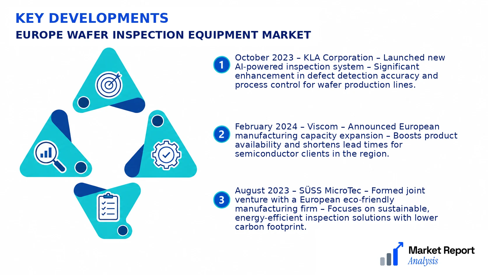
- October 2023 – KLA Corporation – Launched new AI-powered inspection system – Significant enhancement in defect detection accuracy and process control for wafer production lines.
- February 2024 – Viscom – Announced European manufacturing capacity expansion – Boosts product availability and shortens lead times for semiconductor clients in the region.
- August 2023 – SÜSS MicroTec – Formed joint venture with a European eco-friendly manufacturing firm – Focuses on sustainable, energy-efficient inspection solutions with lower carbon footprint.
- January 2024 – Camtek – Initiated acquisition of a European detection technology startup – Strengthens its portfolio in laser defect review and automation software capabilities.
- April 2024 – Nidec-Shimpo – Invested in a new European R&D center – Enhances innovation in surface defect detection technologies using advanced imaging and AI.
Frequently Asked Questions
What is the Europe Wafer Inspection Equipment Market?
The Europe Wafer Inspection Equipment Market encompasses the industry involved in manufacturing and deploying advanced inspection tools designed to detect defects and ensure quality in semiconductor wafers. It supports the broader electronics and semiconductor sectors within Europe.
What is the current market size of Europe Wafer Inspection Equipment Market?
As of 2026, the market is valued at approximately USD 4.5 Billion, reflecting ongoing demand driven by technological advancements and adoption in semiconductor manufacturing facilities across Europe.
What factors are driving the Europe Wafer Inspection Equipment Market?
Growth is fueled by increasing semiconductor production, technological innovation in inspection tools, stringent quality standards, and rising investments from semiconductor manufacturers seeking higher yields and defect detection capabilities.
Which region dominates the Europe Wafer Inspection Equipment Market?
Western Europe leads the market, driven by its mature semiconductor industry, high technological adoption rates, and heavy investments from industry giants located in Germany, France, and the UK.
Which segment is expected to grow the fastest?
Automated inspection systems are projected to exhibit the fastest growth, owing to their enhanced accuracy, efficiency, and capability to handle high-volume wafer production environments.
Who are the leading companies operating in the Europe Wafer Inspection Equipment Market?
Major players include KLA Corporation, Advantest Corporation, and Hermes Microvision, Inc., which are investing heavily in R&D to develop innovative solutions and expand their market shares across the European region.
Analyst Perspective
The Europe Wafer Inspection Equipment Market is poised for robust growth through 2034, driven by technological advancements and increasing demand for higher precision in semiconductor manufacturing. Long-term market outlook suggests sustained expansion, with a focus on automation and AI-enabled inspection systems that enhance defect detection efficiency. Commercial opportunities will predominantly lie in deploying integrated inspection solutions that cater to advanced node technologies and emerging applications such as IoT and 5G. Technological evolution will likely prioritize real-time defect analytics and miniaturization of equipment to accommodate wafer size and complexity. Investment strategies should emphasize R&D, particularly in machine learning algorithms and hardware miniaturization, to stay ahead of competitive pressures. The region’s growth potential is high, especially with Europe’s push toward semiconductor sovereignty and increased governmental funding. Competitive intensity is expected to intensify as global players expand locally, creating opportunities for strategic partnerships. Long-term, market leaders will need to balance technological innovation with regional regulatory and supply chain considerations to secure sustainable growth.
