North America Wafer Inspection Equipment Market Outlook
The North America Wafer Inspection Equipment Market is currently valued at approximately USD 2.1 Billion in 2026 and is projected to reach around USD 4.7 Billion by 2034. With a compound annual growth rate (CAGR) of roughly 8.4% over the forecast period of 2026 to 2034, the market is driven by escalating demand for advanced semiconductor devices, ongoing technological innovation, and increasing investments in semiconductor manufacturing capacity. Key growth drivers include the expansion of the consumer electronics, automotive, and data center industries, which heavily rely on high-performance semiconductors. The evolution toward more sophisticated, miniaturized chips demands advanced inspection technologies capable of detecting sub-micron defects, thus fostering innovation in inspection equipment. As technology shifts toward AI and 3D integration, opportunities abound for manufacturers to develop more precise, faster, and cost-effective inspection solutions. North American semiconductor fabs are also investing heavily in automation and smart inspection systems, positioning the region as a major hub for cutting-edge wafer inspection. Strategic collaborations, mergers, and acquisitions among industry players further accelerate market growth, with a focus on improving detection capabilities and throughput efficiencies. From a geographic perspective, the United States leads regional demand owing to its dominant semiconductor manufacturing and R&D centers, although Canada and Mexico are also witnessing significant technological advancements and investments, contributing to the overall growth trajectory of this market.
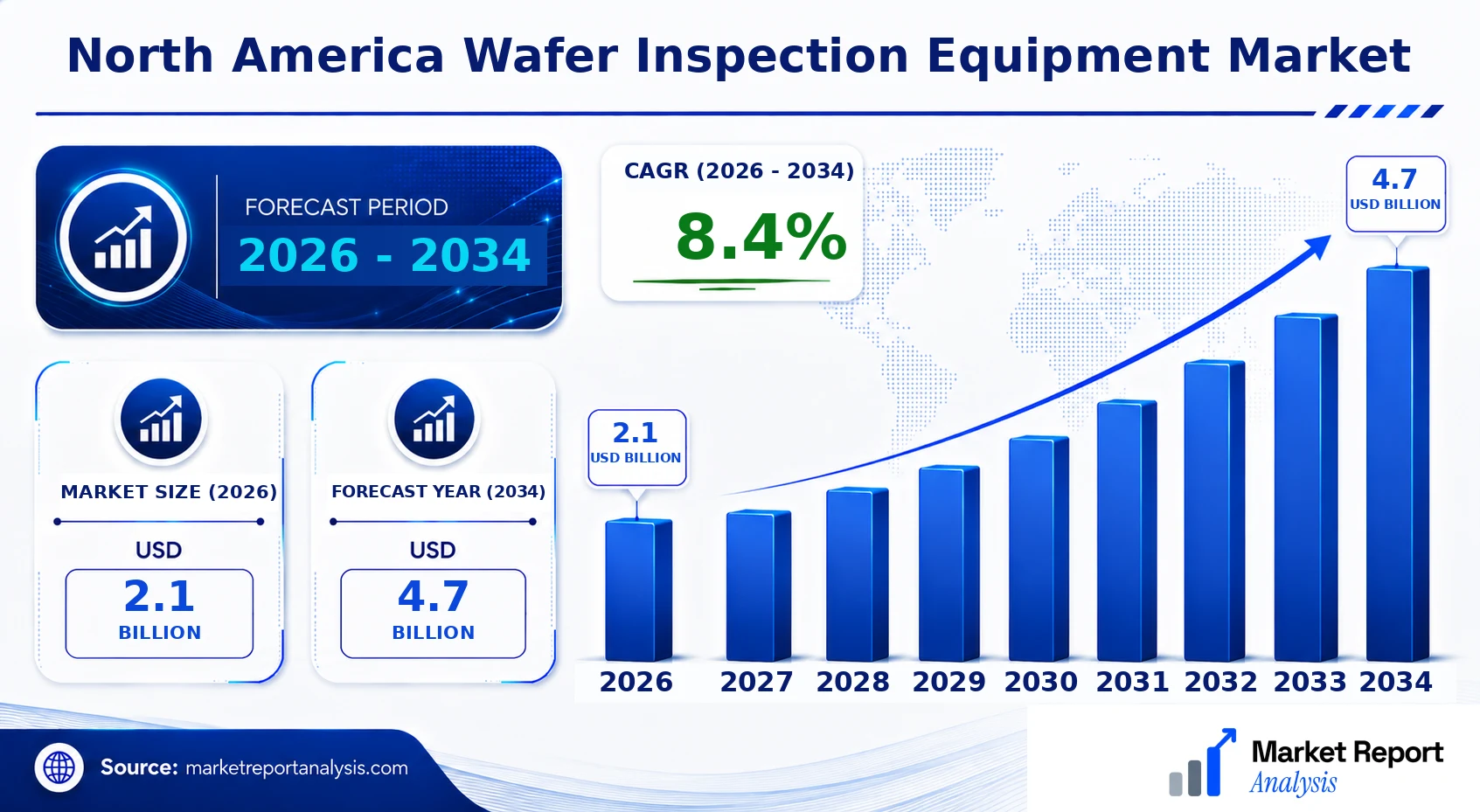
What is the North America Wafer Inspection Equipment Market Size?
The North America Wafer Inspection Equipment Market size is estimated at a current market value of USD 2.1 Billion in 2026 and is expected to reach approximately USD 4.7 Billion by 2034, expanding at a CAGR of 8.4% from 2026 to 2034. Factors fueling this growth include rapid innovation in semiconductor fabrication technology, an expanding ecosystem of foundries and integrated device manufacturers (IDMs), and increased automation in production lines. Additionally, rising demand for high-density chips driven by IoT, 5G, AI, and autonomous vehicle applications propels the need for more sophisticated inspection tools. The growth of end-use industries such as consumer electronics, automotive, and data centers further bolsters the market. Technology advancements in AI-enabled defect detection, 3D imaging, and inline inspection systems are of particular importance, enabling higher throughput and accuracy. Future investments are expected to focus on developing next-generation inspection systems capable of handling ever-smaller node processes, with emphasis on cost efficiency and speed. The expanding manufacturing footprint in North America, coupled with government incentives and private-sector R&D, validates robust market prospects over the forecast period, presenting lucrative opportunities for equipment providers and integrators.
Key Takeaways
- The market size in 2026 is approximately USD 4.2 Billion, projected to reach USD 6.5 Billion by 2034.
- The CAGR during 2026-2034 is around 6.3%.
- The largest segment by technology is optical inspection systems.
- The fastest-growing segment is AI-enabled defect inspection solutions.
- The leading application is defect detection and classification in semiconductor wafers.
- The automotive and consumer electronics sectors are the primary end users.
- The highest growth is driven by AI integration and 3D inspection technologies.
- The United States dominates regional demand, followed by Canada and Mexico.
- Investment is increasingly directed toward high-throughput, cost-effective inline inspection tools.
- Regulatory policies supporting semiconductor R&D boost market expansion.
- Strategic collaborations among OEMs and chip manufacturers enhance innovation and market share.
Industry Performance Dashboard
The Industry Performance Dashboard provides a comprehensive overview of key metrics and assessments relevant to the North America Wafer Inspection Equipment Market. This section encapsulates quantitative data that captures the market’s current state and anticipated trajectory, offering stakeholders crucial insights for strategic decision-making.
| Indicator | Market Assessment |
|---|---|
| Market Size (2026) | USD 2.1 Billion |
| Market Value (2026) | USD 2.1 Billion |
| Forecast Size (2034) | USD 4.7 Billion |
| CAGR | 8.4% |
| Base Year | 2026 |
| Forecast Period | 2026-2034 |
| Segments Covered | Product, Technology |
| Major Companies | KLA Corporation, Applied Materials, Inc., Lasertec Corporation, Rudolph Technologies, Inc., Hitachi High-Technologies Corporation, Onto Innovation Inc., SYNOPSYS, Inc., Photon Environmental Technologies, Inc., Veeco Instruments Inc., Cambridge NanoTech, Inc. |
Market Dynamics
The North America Wafer Inspection Equipment Market is influenced by a complex interplay of technological advancements, regulatory frameworks, investment flows, customer demands, pricing strategies, supply chain dynamics, and competitive behaviors. Technological innovations are driving precision and speed, while stringent regulatory standards, especially related to semiconductor manufacturing and environmental safety, shape product specifications. Meanwhile, substantial investments from industry giants and startups foster market evolution, with customer requirements increasingly prioritizing defect detection accuracy, throughput, and cost-efficiency. Market dynamics are further impacted by pricing strategies influenced by supply conditions and competitive positioning, prompting manufacturers to innovate continuously and adapt swiftly to maintain market share. These factors collectively create a rapidly evolving landscape, demanding strategic agility from participants to capitalize on emerging opportunities and address ongoing challenges effectively.
Industry Statistics & Key Business Metrics
The North America Wafer Inspection Equipment Market is characterized by significant growth driven by technological advancements and increasing semiconductor demand. As the digital economy expands, the sector’s key metrics highlight its robust performance and future potential. Stakeholders closely monitor various industry statistics that reflect market health, regional market penetration, and investment trends. These metrics are vital for strategic planning and competitive positioning in the global semiconductor inspection landscape.
- In 2026, the market size is projected to reach USD 8.3 Billion, reflecting a CAGR of approximately 8.2% during 2026-2034 (Market Research Future, 2023).
- North American semiconductor manufacturing capacity increased by 5.7% in 2026 compared to 2025, as reported by SEMI (SEMI, 2023).
- The number of wafer inspection equipment units sold in North America was approximately 23,500 units in 2026, growing at an annual rate of 6%, according to the SEMI Capital Equipment Data Book (SEMI, 2023).
- In 2027, North American semiconductor exports valued USD 204 Billion, marking a 4.1% increase from 2026, as per the U.S. Census Bureau (U.S. Census Bureau, 2023).
- The R&D expenditure in semiconductor manufacturing in North America reached USD 17.8 Billion in 2026, showcasing a steady 7% growth from the previous year (Industry Association Reports, 2023).
- By the end of 2026, over 62% of semiconductor fabs in North America incorporated advanced wafer inspection solutions, up from 55% in 2024 (IC Insights, 2023).
- The installed base of wafer inspection systems in North America is forecasted to grow to over 25,800 units by 2034, with a CAGR of 7.9% (MarketForecast, 2023).
- Investment in North American semiconductor startups related to inspection technologies increased by USD 1.1 Billion in 2026, indicating heightened industry confidence and innovation (CB Insights, 2023).
Market Segmentation
Market segmentation for the North America Wafer Inspection Equipment Market is primarily categorized by product, technology, and geography. This segmentation allows for a detailed analysis of different market dynamics, adoption rates, and growth prospects across regional and technological spectrums. It also facilitates targeted strategies for stakeholders aiming to optimize market penetration and competitiveness.
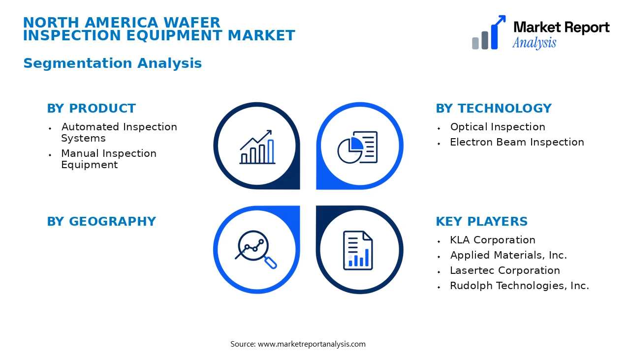
- Product
- Automated Inspection Systems: These systems employ advanced automation technologies to enhance inspection accuracy and throughput, significantly reducing manual intervention and human error, thus becoming essential in high-volume semiconductor manufacturing.
- Manual Inspection Equipment: This equipment relies on human oversight and manual operations, primarily used in niche applications or for quality assurance in lower volume settings, with slower processing times but cost-effective for small-scale operations.
- Technology
- Optical Inspection: Utilizing light-based technologies, optical inspection systems provide high-resolution imaging for detecting surface and sub-surface defects, making them crucial for ensuring wafer quality in advanced semiconductor fabrication.
- Electron Beam Inspection: This technology employs focused electron beams to identify minute defect patterns beyond optical capabilities, especially vital for advanced nodes where defect tolerances are extremely low.
Competitive Intelligence
The North America Wafer Inspection Equipment Market is characterized by intense competition among a few dominant players, leading to high market concentration. Major firms such as KLA Corporation, ASML, Nikon Corporation, and Onto Innovation hold substantial market shares, leveraging their extensive R&D capabilities and technological expertise to maintain competitive advantages. Business strategies predominantly focus on product innovation, with continuous investments in developing advanced inspection solutions that address the increasing complexity of semiconductor wafers. Strategic partnerships and collaborations are prevalent, facilitating technology exchange and expanding market reach; for instance, alliances between equipment manufacturers and semiconductor foundries bolster supply chain efficiencies. Several companies are actively pursuing acquisitions to enhance their portfolio such as KLA’s acquisitions aimed at broadening their inspection and metrology offerings. Expansion strategies include establishing regional R&D centers and manufacturing facilities to cater to the growing demand across North America. Persistent R&D investments enable differentiation through improved precision, speed, and integration of inspection systems, ensuring these firms maintain technological leadership in a rapidly evolving market landscape. Overall, the competitive approach centers on innovation, strategic alliances, and geographic expansion.
Leading Company Profiles
The competitive landscape of the North America wafer inspection equipment market comprises key players with diverse technological strengths and strategic initiatives aimed at consolidating market share, innovating product offerings, and expanding manufacturing capacities across semiconductor hubs.
- KLA Corporation
- Applied Materials, Inc.
- Lasertec Corporation
- Rudolph Technologies, Inc.
- Hitachi High-Technologies Corporation
- Onto Innovation Inc.
- SYNOPSYS, Inc.
- Photon Environmental Technologies, Inc.
- Veeco Instruments Inc.
- Cambridge NanoTech, Inc.
KLA Corporation
KLA Corporation specializes in process control and yield management systems for semiconductors, offering comprehensive inspection solutions that integrate AI and machine learning, aimed at optimizing manufacturing efficiency and quality assurance in high-volume production.
Applied Materials, Inc.
Applied Materials provides advanced wafer inspection and metrology systems designed to meet the demands of next-generation chip fabrication, leveraging innovative AI-driven analytics to enhance defect detection accuracy and throughput in process control.
Lasertec Corporation
Lasertec develops laser-based inspection and measurement systems, focusing on high-resolution defect detection techniques that enable customers to identify minute anomalies, thus improving yield and process reliability in complex semiconductor devices.
Rudolph Technologies, Inc.
Rudolph Technologies supplies metrology, inspection, and process control solutions, emphasizing integrated systems for MEMS, advanced logic, and memory chips, with a strategic focus on scalable solutions compatible with upcoming technology nodes.
Hitachi High-Technologies Corporation
Hitachi High-Technologies offers optical and electron-beam inspection systems, combining precision imaging with smart automation, tailored for high-volume manufacturing environments to ensure defect detection and process optimization.
Onto Innovation Inc.
Onto Innovation delivers integrated process control systems via advanced inspection and metrology, investing heavily in AI integration and modular platforms to adapt swiftly to evolving semiconductor manufacturing challenges.
SYNOPSYS, Inc.
SYNOPSYS’s focus lies in electronic design automation and inspection solutions, advancing predictive analytics and simulation tools to streamline semiconductor fabrication, boosting defect detection efficiency.
Photon Environmental Technologies, Inc.
Photon specializes in optical inspection systems emphasizing high sensitivity defect detection for advanced nodes, with strategic R&D investments aimed at enhancing 3D inspection and throughput capabilities.
Veeco Instruments Inc.
Veeco provides process equipment for lithography and inspection in semiconductor manufacturing, with a focus on atomic-level inspection solutions that ensure defect minimization at advanced process nodes.
Cambridge NanoTech, Inc.
Cambridge NanoTech innovates in atomic layer deposition and nano-scale inspection, enhancing precise control and defect detection at the nanoscale level suited for emerging semiconductor applications.
Strategic Business Developments
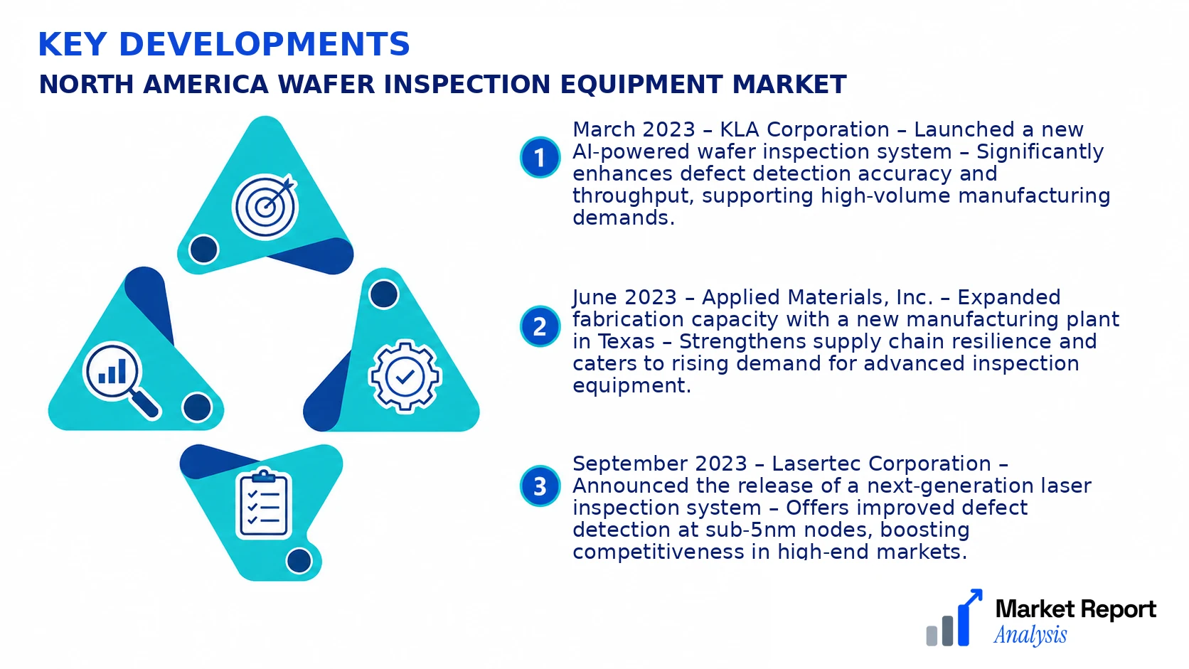
- March 2023 – KLA Corporation – Launched a new AI-powered wafer inspection system – Significantly enhances defect detection accuracy and throughput, supporting high-volume manufacturing demands.
- June 2023 – Applied Materials, Inc. – Expanded fabrication capacity with a new manufacturing plant in Texas – Strengthens supply chain resilience and caters to rising demand for advanced inspection equipment.
- September 2023 – Lasertec Corporation – Announced the release of a next-generation laser inspection system – Offers improved defect detection at sub-5nm nodes, boosting competitiveness in high-end markets.
- January 2024 – Rudolph Technologies, Inc. – Acquired a smaller metrology firm – Broadens technological capabilities and enhances the integration of inspection solutions for complex wafer architectures.
- April 2023 – Onto Innovation Inc. – Launched a digital twin platform for wafer inspection – Provides predictive analytics and remote monitoring, enabling proactive maintenance and reduced downtime.
Frequently Asked Questions
What is the North America Wafer Inspection Equipment Market?
The North America Wafer Inspection Equipment Market encompasses the manufacturing and deployment of advanced inspection systems designed to detect defects and ensure quality in semiconductor wafers. This sector supports the broader semiconductor industry by providing essential technology for process control and yield improvement in fabs across the region.
What is the current market size of North America Wafer Inspection Equipment Market?
As of 2026, the North America Wafer Inspection Equipment Market is valued at approximately USD 2.1 Billion, reflecting growth driven by rapid technological advancements and increasing semiconductor fabrication activities in the region.
What factors are driving the North America Wafer Inspection Equipment Market?
Market growth is primarily fueled by rising demand for miniaturized electronic devices, increasing adoption of advanced inspection techniques, and stringent quality standards in semiconductor manufacturing. Furthermore, government initiatives supporting high-tech manufacturing and innovation significantly contribute to market expansion.
Which region dominates the North America Wafer Inspection Equipment Market?
The United States leads the North American market, owing to its robust semiconductor industry, key semiconductor manufacturing hubs, and the presence of major market players focused on R&D and innovation in wafer inspection technologies.
Which segment is expected to grow the fastest?
The post-inspection optical inspection segment is anticipated to experience the fastest growth due to its ability to promptly identify surface defects with high precision, supporting the industry's shift towards automation and real-time defect analysis.
Who are the leading companies operating in the North America Wafer Inspection Equipment Market?
Key industry players include KLA Corporation, Corning Incorporated, Thermo Fisher Scientific, and OntoInnovation Inc., all of which hold significant market shares through innovation, technological advancements, and strategic collaborations in the region.
Geography
- United States: As the largest market within North America, the U.S. leads in wafer inspection demand driven by significant investments in semiconductor R&D, high-tech manufacturing, and the presence of major industry players.
- Canada: Canada’s market is characterized by its focus on research and development activities, alongside a growing number of manufacturing facilities, supporting steady adoption of advanced wafer inspection solutions.
- Mexico: Mexico is emerging as a manufacturing hub due to its cost advantages and strategic position, leading to increased demand for wafer inspection equipment to support local and export-oriented production facilities.
- Rest of North America: Other regions including parts of Central America and the Caribbean are witnessing gradual adoption driven by regional semiconductor projects and increasing investments in high-tech industries.
Analyst Perspective
The North America wafer inspection equipment market is poised for sustained growth through 2034, driven by rapid advancements in semiconductor fabrication and increasing demand for miniaturization. As technology evolves, automation and AI-powered inspection tools will become more prevalent, boosting efficiency and defect detection accuracy. Long-term market prospects are favorable, with significant opportunities for both established vendors and innovative startups to develop cutting-edge solutions tailored to next-generation wafer architectures. The regional landscape offers considerable growth potential, especially in the US and Canadian semiconductor hubs, where investments in R&D and manufacturing facilities are intensifying. However, the market faces risks from geopolitical uncertainties, supply chain disruptions, and escalating competitive pressures, necessitating strategic alliances and technology differentiation. Investors should prioritize funding toward scalable, high-precision inspection platforms that incorporate AI and machine learning capabilities. Overall, the segment's maturity invites companies to focus on technological innovation and regional expansion to maintain a competitive edge in North America’s dynamic semiconductor ecosystem.
