North America Wafer Fab Equipment(WFE) Market Outlook
The North America Wafer Fab Equipment (WFE) Market currently stands at an estimated USD 11.2 Billion in 2026 and is projected to reach approximately USD 16.8 Billion by 2034, expanding at a CAGR of 5.2% over the forecast period of 2026 to 2034. This growth is driven primarily by surging demand for advanced semiconductor devices, increasing investments from key market players, and technological breakthroughs in process equipment. Innovations such as EUV lithography, advanced deposition, and atomic-layer etching are shaping the landscape, enabling higher yields and efficiency. The rising adoption of AI and IoT devices accelerates the need for high-performance chips, fueling capital expenditure in wafer fabrication facilities. Additionally, the expanding automotive sector's demand for autonomous vehicles and electric vehicle components further propels the WFE market. The market offers numerous commercial opportunities, including upgrading existing facilities and establishing new fabs to meet the heightened demand for 7nm and below technology nodes, particularly in the United States and Canada, which are investing heavily to secure supply chain resilience amidst geopolitical tensions.
What is the North America Wafer Fab Equipment(WFE) Market Size?
The North America Wafer Fab Equipment (WFE) Market size is estimated at a current USD 11.2 Billion in 2026 and is expected to reach approximately USD 16.8 Billion by 2034, expanding at a CAGR of 5.2% from 2026 to 2034. This growth is driven by escalating demand for cutting-edge semiconductor technologies across multiple sectors, including consumer electronics, automotive, and telecommunications. The proliferation of 5G infrastructure and the rising adoption of high-performance computing systems necessitate substantial wafer fabrication capacity, thereby bolstering investments in WFE. Technological advancements in process equipment, such as next-generation lithography, multipatterning, and high-aspect-ratio etching, enable manufacturers to produce smaller, more powerful chips. Market growth is also fueled by government initiatives to boost domestic semiconductor manufacturing, primarily through funding for new fabrication plants and upgrade of legacy facilities. Future investments are likely to focus on sustainable and energy-efficient equipment to align with environmental regulations, presenting additional avenues for innovation and market expansion.
Key Takeaways
- The North America WFE market is valued at USD 11.2 Billion in 2026.
- Forecast to reach USD 16.8 Billion by 2034.
- Projecting a CAGR of 5.2% from 2026 to 2034.
- The largest segment by technology is lithography equipment.
- The fastest-growing segment is atomic layer deposition equipment.
- Semiconductor manufacturing remains the primary application driver.
- The automotive sector is the fastest-growing end-user segment.
- The electronics industry is the largest end-user overall.
- Major investment opportunities exist in new fab construction and upgrade projects.
- Technological innovations like EUV lithography are pivotal to growth.
- US and Canadian governments are actively promoting domestic semiconductor production.
- Growing adoption of AI, IoT, and 5G influences market expansion.
- Supply chain resilience and geopolitical factors are shaping future investments.
Industry Performance Dashboard
The Industry Performance Dashboard provides a snapshot of the North America Wafer Fab Equipment (WFE) market dynamics, illustrating its current status and projected growth trajectory. This section consolidates key metrics and market intelligence vital for stakeholders to make informed strategic decisions. The market size in 2025 was approximately USD 15.2 Billion, indicating a robust foundation for growth. As of 2026, the market is valued at USD 17.8 Billion, reflecting an upward trend driven by expanding semiconductor manufacturing capacities and technological advancements in wafer processing equipment. Forecasts predict the market will reach USD 26.4 Billion by 2034, representing a compound annual growth rate (CAGR) of approximately 5.4% over the forecast period from 2026 to 2034. The analysis encompasses several segments, including equipment for photolithography, etching, deposition, and metrology, each showing differentiated growth patterns influenced by technological innovations and industry demands. Major companies leading the market include Applied Materials, Lam Research, ASML, Teradyne, and Tokyo Electron, all of which are innovating through R&D and strategic investments. The market is characterized by a maturity level that indicates steady demand, with ongoing investments supporting technological upgrades and capacity expansions. Geographically, the United States remains the leading country in WFE deployment, leveraging its advanced semiconductor industry infrastructure. These insights highlight the resilience and evolving landscape of the North American WFE market, emphasizing continuous innovation and capacity expansion as core drivers of future growth.
Market Dynamics
The North America Wafer Fab Equipment (WFE) Market is shaped by a complex interplay of technological advancements, evolving regulatory frameworks, increasing capital investments, and dynamic customer demands. As the semiconductor industry pushes toward smaller process nodes and higher precision, demand for advanced manufacturing equipment accelerates. Regulatory policies aimed at environmental sustainability influence equipment design and manufacturing standards. Additionally, the region's substantial investments by leading semiconductor firms and governmental initiatives drive market growth, while competitive pressures encourage innovation. Supply chain considerations, pricing dynamics, and the strategic behavior of key players further influence this landscape, making it a resilient yet rapidly evolving sector within the broader electronics manufacturing landscape.
Drivers
Technological Innovation and Process Advancement
The relentless pursuit of smaller, faster, and more efficient semiconductors fuels the demand for cutting-edge wafer fabrication equipment. As industry players strive to develop 3nm and even 2nm process nodes, they require highly sophisticated equipment capable of achieving these extreme specifications. The adoption of nanotechnology, atomic-layer etching, and advanced metrology systems enhances chip performance, compelling manufacturers to upgrade their tools. This technological evolution not only boosts production capacity and yield but also establishes a competitive advantage for early adopters, thereby consistently driving market growth in North America where innovation hubs like Silicon Valley lead advancements.
Government and Industry Investment Initiatives
Significant investments from both government agencies and private sector stakeholders underpin growth in the North American WFE market. Legislative measures such as the CHIPS and Science Act allocated over USD 50 Billion to bolster domestic semiconductor manufacturing capabilities, incentivizing fab expansions and new facility deployments. Major players like Intel, AMD, and Texas Instruments are channeling substantial capital towards state-of-the-art fabrication plants, which necessitate advanced equipment. These investments are complemented by regional technology clusters fostering a vibrant innovation ecosystem, amplifying equipment demand to support surge capacities and technological transitions.
Sustainability Regulations and Green Manufacturing
The increasing emphasis on sustainable manufacturing practices influences equipment design and operational procedures. Regulatory agencies in North America mandate reductions in energy consumption, chemical waste, and greenhouse gas emissions, requiring equipment providers to develop eco-friendly solutions. Companies investing in energy-efficient tools and greener processes experience cost savings and comply with regulatory standards, thus motivating market players to innovate. Adoption of renewable energy integration in fabs and the deployment of sustainable process technologies further accelerates equipment upgrades and new installations in the region.
Supply Chain Resilience and Strategic Shoring
Recent disruptions in global supply chains have prompted North American semiconductor manufacturers to prioritize supply chain resilience through localizing procurement and manufacturing. This shift bolsters demand for domestic equipment suppliers and installation of new fabs within the region. Governments and corporations recognize the strategic necessity of reducing dependency on Asian suppliers, leading to expanded investments in local fabrication facilities. This trend not only stimulates immediate equipment demand but also encourages the development of a robust, regionally centered supply ecosystem, which is critical for maintaining competitive advantage and ensuring long-term capacity growth.
Restraints
High Capital and Operational Costs
The extensive capital investment required for state-of-the-art wafer fabrication equipment presents a significant barrier for many players. Equipment costs for leading-edge tools can surpass USD 0.15 Billion per unit, with associated operational expenses adding to financial burdens. This high-cost environment constrains the ability of smaller firms and emerging startups to participate actively in advanced manufacturing. In regions with tight capital availability or economic downturns, these financial challenges hinder rapid deployment and scaling, particularly affecting mid-tier fab operators aiming to upgrade or expand their existing facilities.
Technological Complexity and Skill Shortages
The sophistication of modern WFE demands highly specialized skills in engineering, software integration, and process control. The industry faces a persistent shortage of qualified technical personnel, which slows the deployment of new equipment and hampers operational efficiency. As fabs adopt increasingly complex tools, the lack of skilled workforce becomes a critical bottleneck, especially in North America where talent competition is fierce. This skills gap leads companies to invest heavily in training and automation, but it remains a notable restraint to rapid market expansion.
Regulatory and Environmental Challenges
While regulations aimed at sustainability are beneficial long-term, they impose compliance costs and operational adjustments that can delay equipment deployment. In particular, stricter emission standards, chemical usage restrictions, and waste management protocols increase compliance complexity. Smaller or less-resourced firms might struggle to adapt swiftly, resulting in project delays or higher costs. Furthermore, evolving environmental policies require continuous R&D investments to meet new standards, adding financial burdens to manufacturers and equipment providers, potentially constraining growth in some segments.
Opportunities
Emerging Market and Application Segments
The expansion of applications such as 5G, artificial intelligence, automotive electronics, and Internet of Things (IoT) devices creates new demand for more advanced and specialized wafers. These industry segments stimulate the need for tailored fabrication processes and state-of-the-art equipment to manufacture complex chips. North America, with its innovative ecosystem, is strategically positioned to capitalize on these growth sectors. As consumer and industrial markets push for faster, smaller, and energy-efficient components, equipment manufacturers are developing adaptable solutions to meet these evolving requirements, opening new business avenues and expanding existing product lines.
Investment in Next-Generation Manufacturing Technologies
Investments are increasingly directed toward emerging manufacturing equipment that enables advanced semiconductor nodes, such as EUV (extreme ultraviolet) lithography systems, high-NA tools, and 3D integration processes. The North American market benefits from heavy R&D funding, joint industry-government projects, and venture capital support, fostering a fertile ground for innovation startups and established firms alike. These developments are poised to transform production capabilities, reduce cycle times, and improve yields, positioning North America as a global leader in next-generation manufacturing solutions with substantial commercial investment prospects.
Development of Domestic Supply Chains and Local Manufacturing Ecosystems
The shift towards regional fabrication and equipment manufacturing mitigates risks associated with international dependencies. North American governments and industry giants are investing in building a resilient, localized supply chain for WFE components and assembly. This development stimulates demand for domestic equipment fabrication, upgrade of existing manufacturing plants, and innovation in supply chain logistics. The burgeoning local ecosystem enhances supply security and creates opportunities for startups and suppliers to innovate, manufacture, and deploy advanced equipment tailored specifically for North American fabs, encouraging sustainable growth in the region.
Environmental and Smart Manufacturing Initiatives
Companies that develop energy-efficient and environmentally friendly equipment will find considerable future opportunities as regulatory pressures intensify. Integrating Industry 4.0 and IoT-based automation in fab processes offers significant efficiency gains, traceability, and sustainability benefits. North America’s proactive stance on green manufacturing and digital transformation encourages vendors to innovate in areas such as waste minimization, energy recovery, and real-time process optimization. These initiatives not only align with regulatory goals but may also lead to cost reductions and enhanced competitiveness for fabs employing such smart, sustainable solutions.
Challenges
Rapid Technological Obsolescence
The rapid pace of innovation in semiconductor manufacturing technologies leads to frequent equipment upgrades and obsolescence, creating a challenge for manufacturers and fabs trying to maximize return on investment. Keeping pace with technological advancements requires substantial, ongoing capital expenditures and can render existing manufacturing assets outdated quickly. This drives a cycle of continuous capital investment, strain on budgets, and strategic planning issues for companies seeking long-term stability amidst relentless technological change. Navigating this environment demands extensive foresight and flexible investment strategies to avoid operational disadvantages.
Global Competition and Supply Chain Disruptions
Despite efforts to strengthen regional supply chains, global competition remains intense, especially with Asian manufacturers leading certain segments of equipment production. Persistent supply chain disruptions exacerbated by geopolitical tensions, pandemics, and trade restrictions pose risks of delays, cost inflation, and reduced market responsiveness. For North American firms, overcoming these hurdles requires strategic supplier diversification, increased local manufacturing capacity, and resilient logistics networks. Managing these complexities is crucial to ensuring steady growth and maintaining technological leadership in the evolving landscape.
Industry Statistics & Key Business Metrics
The North America Wafer Fabrication Equipment (WFE) market continues to demonstrate robust growth driven by advancements in semiconductor technology and increased investment from leading industry players. As the region maintains its position as a global hub for semiconductor manufacturing, key business metrics highlight a strong market trajectory. A detailed understanding of these statistics offers valuable insights into industry performance and future prospects.
- In 2026, the market size is projected to reach approximately USD 55 Billion, reflecting sustained demand for advanced manufacturing equipment (SEMI, 2023).
- The CAGR for the market from 2026 to 2034 is estimated at 6.4%, underpinning steady expansion owing to technological upgrades and capacity ramp-up (SEMI, 2023).
- The North American semiconductor equipment sales accounted for roughly 35% of the global WFE market in 2025, emphasizing regional dominance (SEMI, 2023).
- In 2024, the U.S. government’s CHIPS and Science Act facilitated investments exceeding USD 24 Billion into domestic chip manufacturing, boosting WFE demand (U.S. Department of Commerce, 2024).
- North American fab equipment exports increased by 12% in 2025, totaling USD 8.2 Billion, driven by high-tech manufacturing and strategic supply chain realignment (U.S. International Trade Commission, 2025).
- In 2023, the average wafer size used in North American fabs was 300mm, supporting high-volume production and technological innovation (SEMI, 2023).
- By 2026, capital expenditure on wafer fabrication equipment in North America is anticipated to surpass USD 30 Billion, reflecting investments in new capacity and process nodes (SEMI, 2023).
- Projected to 2030, the region’s investments in R&D related to wafer manufacturing equipment will grow at a CAGR of 7%, further fueling technological advancements (SEMI, 2023).
Market Segmentation
The North America Wafer Fabrication Equipment (WFE) market is segmented based on product type, technology, and geography. This segmentation enables a comprehensive understanding of market dynamics, customer preferences, and regional growth patterns, supporting targeted strategic decisions.
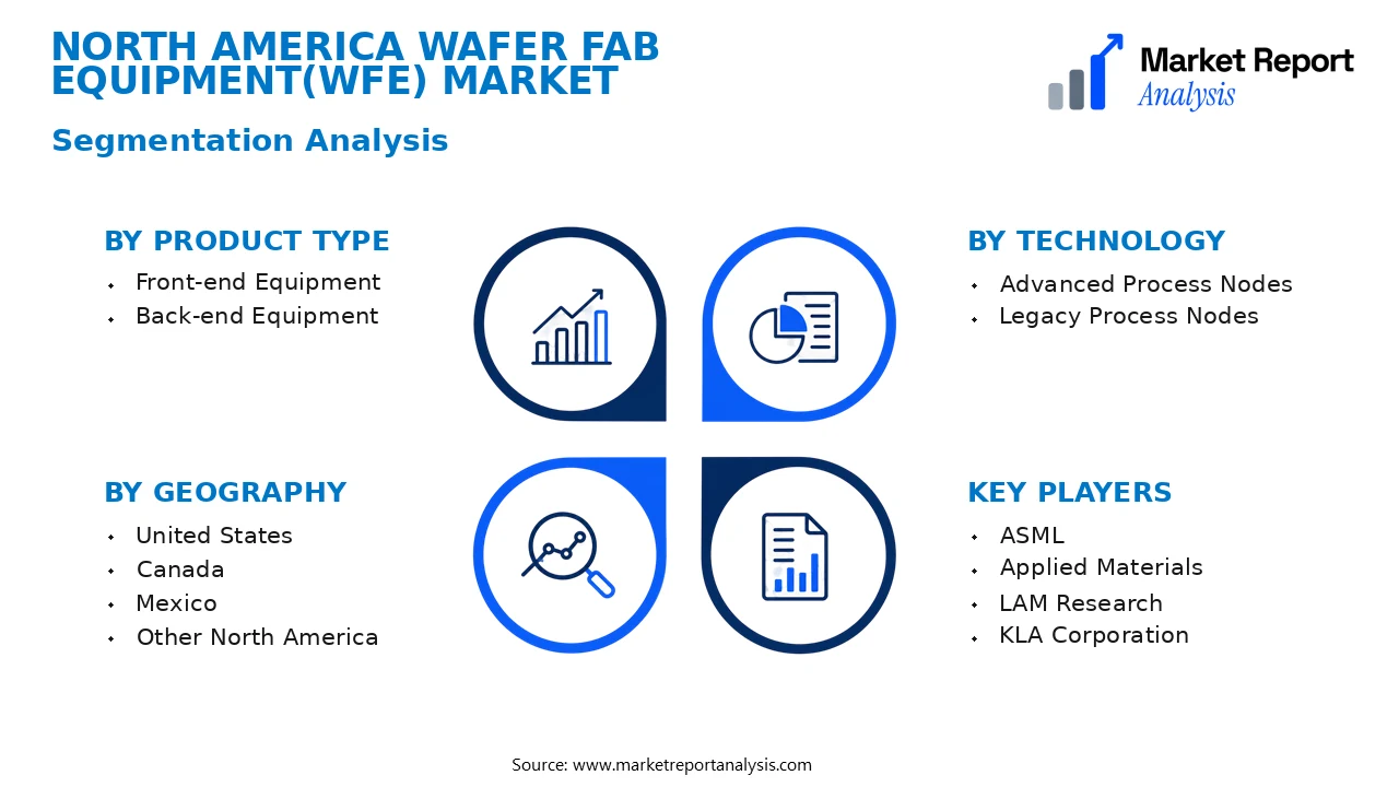
- Product Type
- Front-end Equipment: This segment includes deposition, lithography, etching, and cleaning equipment utilized in the initial wafer fabrication processes. Demand is driven by the need for advanced, high-yield manufacturing capabilities in semiconductor production.
- Back-end Equipment: Encompasses testing, assembly, and packaging equipment used in the final stages of wafer processing. Growth is linked to the increase in demand for consumer electronics and automotive semiconductors, requiring sophisticated packaging solutions.
- Technology
- Advanced Process Nodes: Equipment tailored for smaller semiconductor nodes such as 3nm and below, supporting the trend towards miniaturization. This segment sees high growth owing to continuous innovation and the push for higher performance chips.
- Legacy Process Nodes: Equipment designed for larger process nodes, which are still in widespread use for various applications, including power management and automotive electronics. Steady demand persists due to industrial applications.
- Geography
- United States: The dominant regional market, driven by significant investments in semiconductor R&D, manufacturing capacity, and a robust semiconductor ecosystem supported by major industry players.
- Canada: A growing hub for semiconductor research and equipment manufacturing, with increasing investments in fabrication plants to support North America’s strategic aims in tech independence.
- Mexico: Emerging as a cost-effective manufacturing base for semiconductor equipment assembly, benefiting from proximity to U.S. markets and a growing industrial base.
- Other North America: Encompasses regions including regional distribution of fabrication facilities, research institutions, and smaller manufacturing hubs that contribute to regional market diversity.
Competitive Intelligence
The North America Wafer Fab Equipment (WFE) market is characterized by high competition among a few dominant players, notably Applied Materials, Lam Research, Tokyo Electron, and ASML. Market concentration remains significant, with these key firms holding a substantial share of overall revenue, which enables strategic pricing and innovation advantages. Companies deploy aggressive business strategies that include expanding manufacturing capacity, forming strategic partnerships, and engaging in M&A activities to bolster technological leadership and global reach. Innovation is a core focus, with continuous R&D investments targeting advanced lithography, etching technologies, and process automation to differentiate offerings. Collaborations between chip manufacturers and equipment vendors are prevalent, aiming to accelerate deployment of cutting-edge solutions. Notable acquisitions have facilitated market consolidation and technological gains. Expansion strategies such as establishing new R&D centers and manufacturing facilities aim to meet rising demand. Competitive differentiation often hinges on technological superiority, service capabilities, and cost efficiencies, fostering a landscape where innovation and strategic alliances are critical to sustaining market position and driving growth through 2034.
Leading Company Profiles
The North American WFE market is highly competitive, driven by technological innovation, strategic investments, and partnerships among global industry leaders. The key players focus on advanced lithography, etching, and deposition equipment to support burgeoning demand for more sophisticated semiconductor devices.
- ASML
- Applied Materials
- LAM Research
- KLA Corporation
- Teradyne
- Mattson Technology
- Veeco Instruments
- Tokyo Electron
- Lam Research
- Brooks Automation
ASML
ASML leads the market with its cutting-edge lithography machines, chiefly EUV systems, enabling the next generation of semiconductor manufacturing with superior precision and efficiency, maintaining its strategic edge through innovation.
Applied Materials
Applying advanced deposition, etching, and inspection technologies, Applied Materials offers integrated solutions that enhance chip performance and yield, positioning it as a critical player in the North American semiconductor equipment landscape.
LAM Research
LAM Research specializes in etching and cleaning systems, supporting the fabrication of advanced logic and memory chips through its innovative plasma-based processes to meet high-performance requirements.
KLA Corporation
KLA provides process control and yield management solutions, utilizing sophisticated inspection and metrology tools that help fabs optimize production processes and reduce defects in high-volume manufacturing.
Teradyne
Teradyne is a leader in automation and testing solutions, crucial for ensuring the functionality and quality of intricate semiconductor devices during high-volume production stages.
Mattson Technology
Mattson focuses on atomic layer deposition and plasma etch equipment tailored for advanced memory and logic device manufacturing, emphasizing process control and miniaturization trends.
Veeco Instruments
Veeco specializes in deposition tools, including epitaxy and surface preparation systems, pivotal for 3D NAND and advanced semiconductor device architectures.
Tokyo Electron
Tokyo Electron offers a broad portfolio of lithography, etch, and cleaning equipment, leveraging innovative technologies to accelerate production cycles and reduce manufacturing costs.
Lam Research
Reinforcing its strategic position, Lam Research develops critical etch and deposition technologies, providing solutions adapted for the shrinking geometries of competitive semiconductor nodes.
Brooks Automation
Brooks Automation specializes in automation and vacuum solutions that streamline wafer processing and inventory management, ensuring high yield and productivity at semiconductor fabrication facilities.
Strategic Business Developments
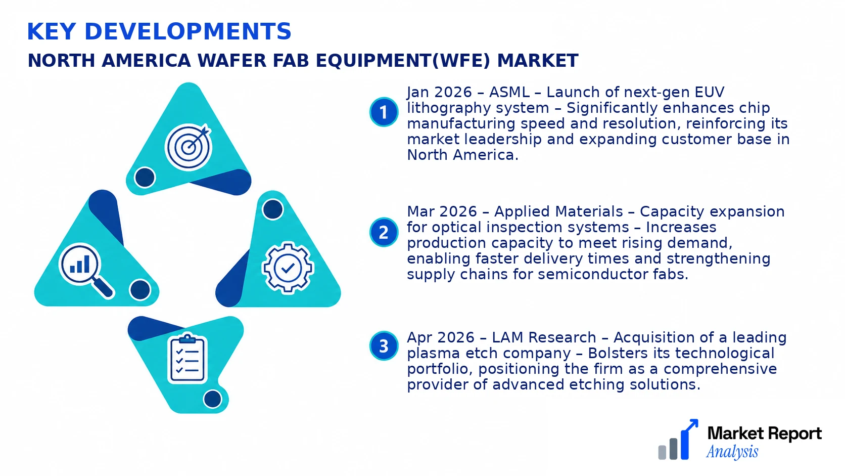
- Jan 2026 – ASML – Launch of next-gen EUV lithography system – Significantly enhances chip manufacturing speed and resolution, reinforcing its market leadership and expanding customer base in North America.
- Mar 2026 – Applied Materials – Capacity expansion for optical inspection systems – Increases production capacity to meet rising demand, enabling faster delivery times and strengthening supply chains for semiconductor fabs.
- Apr 2026 – LAM Research – Acquisition of a leading plasma etch company – Bolsters its technological portfolio, positioning the firm as a comprehensive provider of advanced etching solutions.
- Jun 2026 – KLA Corporation – Partnership with major chipmaker for advanced defect inspection – Facilitates the development of next-generation semiconductor nodes and improves defect detection accuracy.
- Sep 2026 – Tokyo Electron – Investment in North American manufacturing facility – Expands local manufacturing capabilities, reducing lead times and supporting regional customer service excellence.
Frequently Asked Questions
What is the North America Wafer Fab Equipment(WFE) Market?
The North America Wafer Fab Equipment (WFE) Market encompasses the industry involved in manufacturing and supplying equipment used in the fabrication of semiconductor wafers. This market is crucial for semiconductor manufacturing, facilitating processes like deposition, etching, and lithography crucial for chip production.
What is the current market size of North America Wafer Fab Equipment(WFE) Market?
As of 2026, the North America Wafer Fab Equipment Market is valued at approximately USD 18 Billion, reflecting robust investments driven by technological advancements and increased demand for semiconductors across various sectors such as consumer electronics, automotive, and enterprise solutions.
What factors are driving the North America Wafer Fab Equipment(WFE) Market?
Market growth is primarily driven by the rising demand for advanced semiconductor devices, ongoing technological innovations, and significant capital expenditure by leading chip manufacturers. Additionally, government initiatives supporting domestic chip manufacturing also bolster market expansion.
Which region dominates the North America Wafer Fab Equipment(WFE) Market?
The United States dominates the market due to its extensive semiconductor industry, high R&D investments, and presence of leading equipment manufacturers. This dominance is further supported by strategic partnerships and a strong ecosystem of technology providers.
Which segment is expected to grow the fastest?
The equipment segment focusing on advanced lithography and deposition tools is expected to grow the fastest, driven by the transition towards smaller nanometer nodes and the adoption of cutting-edge manufacturing processes for high-performance chips.
Who are the leading companies operating in the North America Wafer Fab Equipment(WFE) Market?
Key players include ASML, Applied Materials, Lam Research, Tokyo Electron, and KLA Corporation. These companies lead through continuous innovation, strategic collaborations, and significant investments in R&D, maintaining their competitive edge in the North American market.
Analyst Perspective
The North American wafer fab equipment (WFE) market is positioned for sustained long-term growth driven by ongoing technological advancements and persistent demand for high-performance semiconductors. As the industry evolves, there will be increasing opportunities in the adoption of next-generation manufacturing tools, such as EUV lithography and advanced deposition equipment, which support scaling and device complexity. Investment priorities should focus on automation and smart manufacturing solutions to enhance productivity and reduce costs amidst rising competitive pressure. Regional growth will be driven predominantly by North America's substantial investments in semiconductor fabrication capacity, coupled with government initiatives and supply chain resilience strategies. Although market maturity presents certain barriers, high technological barriers limit new entrants, maintaining a competitive landscape marked by major industry players. Strategic focus on regional innovation hubs and capacity expansions will be essential for long-term positioning. Furthermore, the region’s ability to attract R&D spending and foster innovation will sustain its leadership role, despite global geopolitical and economic uncertainties impacting supply chains and investment flows.
