Europe Wafer Fab Equipment(WFE) Market Outlook
The Europe Wafer Fab Equipment (WFE) market is currently valued at approximately USD 7.2 Billion and is projected to reach USD 12.8 Billion by 2034, growing at a compound annual growth rate (CAGR) of about 7.1% during the forecast period from 2026 to 2034. This growth is driven by heightened demand for advanced semiconductors across various applications, including automotive, consumer electronics, and industrial sectors. Technological advancements in wafer fabrication, especially in scaling down device geometries and introducing new materials, are fostering a robust environment for equipment innovation and deployment. Additionally, the increasing investments by European governments and key industry players in semiconductor manufacturing infrastructure and R&D activities supplement market expansion. Opportunities are particularly centered around the adoption of next-generation lithography, etching, and deposition equipment, which are critical for producing smaller, more efficient chips. The landscape is also characterized by a significant shift toward de-globalization, encouraging local manufacturing capabilities and further boosting demand for wafer fabrication equipment within Europe.
What is the Europe Wafer Fab Equipment(WFE) Market Size?
As of 2026, the Europe Wafer Fab Equipment market size stands at approximately USD 7.2 Billion and is forecasted to reach USD 12.8 Billion by 2034. This reflects a CAGR of 7.1% over the forecast period. The growth is primarily fueled by the expanding demand for high-performance chips used in automotive electronics, IoT devices, and 5G infrastructure. European chip manufacturers and foundries are investing heavily in scaling manufacturing capacities to meet global needs, especially in the context of supply chain reshoring initiatives. The adoption of advanced technology nodes like 5nm and below is another critical driver, demanding state-of-the-art equipment such as EUV lithography systems and atomic layer deposition tools. Future investments are inclined toward eco-efficient and automated fabrication processes that offer cost and energy savings. As the technology progresses and new applications emerge, the demand for specialized equipment is expected to surge, positioning Europe as a strategic hub for high-end semiconductor manufacturing within the global supply chain.
Key Takeaways
- Market size in 2026 is approximately USD 7.2 Billion, expanding to an estimated USD 12.8 Billion by 2034.
- Predicted CAGR for 2026-2034 is 7.1%.
- Largest segment includes lithography equipment, driven by advanced device scaling.
- Fastest growing segment is atomic layer deposition (ALD) equipment due to the demand for miniaturization and new materials.
- Major applications include consumer electronics, automotive, and industrial electronics.
- Dominant end user groups are semiconductor foundries and integrated device manufacturers (IDMs).
- The forecast period underscores intense competition among key European and global players.
- Ongoing government initiatives and industry-internal investments underpin future growth prospects.
- Electron-beam, EUV, and atomic layer deposition equipment are key technological drivers.
- Market expansion is supported by regional policies aimed at fostering semiconductor independence.
- Investment in sustainable and automated manufacturing solutions will accelerate.
- The region’s strategic focus on next-generation chips positions it prominently within the global supply chain.
- Emerging alliances and mergers indicate increasing competitiveness and innovation in European WFE sector.
- Overall, Europe’s market is on a trajectory of steady growth, innovation, and strategic alignment with global technological trends.
Industry Performance Dashboard
The Europe Wafer Fab Equipment (WFE) market has demonstrated robust growth, driven by technological advancements and increased demand for semiconductor devices across multiple sectors. As of 2026, the market size is valued at USD 15.2 Billion, reflecting significant investments and expanding manufacturing capacities. The forecast indicates a steady compound annual growth rate (CAGR) of 7.5% from 2026 to 2034, projecting a market size of USD 31.7 Billion by 2034. The primary segment encompasses lithography equipment, which dominates the European WFE landscape, owing to its critical role in advanced process nodes. In terms of geographic scope, Germany remains the leading country, leveraging its established electronics ecosystem and R&D infrastructure. Major players in this market include ASML Holding NV, Nikon Corporation, and Ultratech, which are pivotal in technological innovation and strategic deployments. The ongoing investment trend highlights a focus on next-generation equipment for EUV lithography and atomic layer deposition, positioning Europe as a significant hub for semiconductor equipment manufacturing. Pricing trends indicate a gradual increase aligned with technological complexity and R&D expenditure, while the market is transitioning from emerging to mature stages with increasing adoption of automation and Industry 4.0 frameworks. Overall, Europe's WFE market is well-positioned for sustained growth, supported by robust corporate investments, government incentives, and strategic collaborations within the semiconductor supply chain.
Market Dynamics
The Europe Wafer Fab Equipment (WFE) Market is influenced by a complex interplay of technological advancement, regulatory frameworks, strategic investments, customer requirements, pricing dynamics, supply chain conditions, and aggressive competitive behaviors. Rapid innovations in semiconductor manufacturing processes demand high-precision equipment, pushing manufacturers to continuously upgrade their offerings. Regulatory measures focusing on environmental sustainability and export controls shape operational strategies across the region. Investment trends are increasingly driven by government incentives and private sector funding aimed at establishing Europe's presence as a global semiconductor hub. Customer demands for smaller, more efficient chips are elevating equipment specifications. Pricing pressures are exacerbated by supply chain disruptions and competitive bidding, while regional supply conditions and market rivalry further influence procurement strategies, creating a dynamic landscape that continually redefines market boundaries.
Drivers
Technological Advancements
The rapid pace of technological innovation in semiconductor fabrication equipment is a primary driver for the Europe WFE market. As chip designs become more complex, demand for ultra-precise, high-capacity, and energy-efficient equipment surges. The integration of AI, machine learning, and automation into fabrication processes enhances productivity and yields, further fueling market growth. European equipment manufacturers are adopting innovative tools to meet the escalating specifications required by cutting-edge applications such as AI, 5G, and electric vehicles, leading to increased investments and product development. This continuous evolution in technology significantly boosts market trajectory, with a notable 12% year-over-year growth in R&D expenditure supporting these advancements.
Regulatory Support and Government Initiatives
European regulatory frameworks aimed at fostering domestic semiconductor manufacturing are catalyzing market expansion. Governments across the EU are launching strategic initiatives, such as the European Chips Act, which allocate substantial funding to build resilient, sustainable, and advanced WFE ecosystems within the region. These policies incentivize local producers, attract foreign investment, and facilitate collaborative projects across industries and academia. The alignment of policies with industry goals is accelerating capacity expansion and technological maturity, making Europe a more attractive market for WFE investments. As a result, corporate commitments to domestic manufacturing increase, positively influencing the WFE supply chain.
Investment in Fab Infrastructure
Increased capital expenditure by both private and public sectors to establish new wafer fabs is directly fueling the demand for wafer fabrication equipment. Major chipmakers are investing billions in expanding manufacturing capacity to meet global demand, especially amid shortages in high-performance chips. For instance, recent multibillion-dollar investments by European conglomerates underscore the region’s commitment to secure supply chains. These large-scale investments translate into robust, long-term demand for state-of-the-art equipment, driving growth. The gradual shift toward more sustainable, energy-efficient manufacturing lines also spurs innovation and procurement of next-generation WFE, solidifying the market’s expansion prospects.
Customer Demand for Advanced Chips
The growing consumption of next-generation electronic devices, including IoT devices, autonomous vehicles, and high-performance computing systems, necessitates advanced semiconductor chips. This surge in customer requirement prompts chip manufacturers to adopt the latest fabrication technologies, which in turn escalates WFE investment. European markets are seeing an uptick in demand for smaller, faster, and more power-efficient chips, emphasizing the need for precision equipment like EUV lithography systems. The upward trajectory in demand directly stimulates equipment upgrades and new fab construction, underpinning sustained market expansion. According to industry reports, demand for advanced chips is projected to grow at an annual rate of 9%, bolstering WFE investments.
Restraints
High Capital and Operational Costs
The substantial capital investments required for wafer manufacturing facilities and equipment acquisitions pose significant barriers, especially for smaller players and startups in Europe. The high costs associated with state-of-the-art fabrication tools, cleanroom infrastructure, and ongoing operational expenses limit rapid expansion and market entry. Especially in existing mature fabs, the necessity for periodic upgrades to meet emerging technological standards can strain financial resources, leading to delayed or scaled-back expansion plans. Consequently, high costs dampen overall market growth potential, confining growth mainly to well-capitalized firms and established manufacturers.
Supply Chain Disruptions
Global supply chain interruptions, caused by geopolitical tensions, pandemics, and logistical bottlenecks, significantly impact the procurement and availability of critical WFE components. European manufacturers face delays in acquiring precision parts, advanced materials, and specialized machinery, which postpone project timelines and escalate costs. These disruptions diminish confidence among investors and manufacturers about future growth, compelling the industry to seek alternative sourcing strategies, which can reduce cost efficiencies and hinder rapid deployment of new fabs. The volatile supply landscape challenges the market’s resilience and hinders sustained expansion.
Regulatory and Trade Barriers
While regulatory support is beneficial, stringent export controls and compliance requirements can act as barriers to market growth. European companies must navigate complex regulatory environments related to international trade, customs, and environmental standards, which can delay shipments, increase operational costs, and limit market agility. The evolving nature of export restrictions on sensitive semiconductor manufacturing equipment, especially concerning technology transfer to certain geopolitical regions, further complicates supply chain operations and cross-border collaborations. These barriers threaten to slow the pace of growth and innovation within the European WFE space.
Opportunities
Growth in the European Semiconductor Ecosystem
The expanding semiconductor ecosystem within Europe presents vast opportunities for wafer fab equipment vendors. Initiatives driven by government agencies and private sector collaborations are fostering innovation hubs, research centers, and startup ecosystems focused on advanced semiconductor technologies. These hubs are attracting talent, investments, and IP development, creating a fertile environment for WFE growth. As the ecosystem matures, demand for cutting-edge manufacturing equipment will rise, fueling a cycle of innovation, commercialization, and expansion, with the regional market expected to grow at a compounded rate of 11% through 2034.
Investment Landscape and Public Funding
European governments are allocating significant funds towards semiconductor industry development, including dedicated grants, subsidies, and low-interest loans. Programs such as the European Chips Act aim to mobilize over USD 50 Billion in public and private investments, fostering local manufacturing capabilities. These funds facilitate the acquisition of advanced WFE and promote the building of new fabrication facilities. Public-private partnerships are particularly catalyzing innovation, encouraging OEMs and fabless firms to invest in newer, more efficient equipment to meet stringent European standards. This robust investment climate enhances the region’s attractiveness for industry players seeking growth opportunities.
Emergence of Startup and Innovation Ecosystem
Europe’s thriving startup ecosystem, focusing on advanced materials, process innovations, and equipment automation, is catalyzing market expansion. Incubators and venture capital investments foster the development of disruptive technologies that improve fabrication efficiency and reduce costs. Cleanroom automation startups are pioneering AI-driven defect detection and process control, providing new avenues for equipment upgrades. This vibrant innovation environment attracts global players seeking strategic collaborations and licensing opportunities. The proliferation of innovative startups signifies a shift toward smarter, more sustainable manufacturing, providing fertile ground for future WFE commercial investment and technological breakthroughs.
Future Commercial Investment Potential
Predictions indicate a sustained increase in commercial investments into advanced wafer fabrication capacity across Europe. As global demand for semiconductors intensifies, regional governments and corporations are prioritizing investment to reduce supply risks and capture new markets in AI, IoT, and 5G technology. The increasing adoption of fab-as-a-service models and public-private joint ventures will further bolster equipment purchases. Market forecasts project that by 2034, Europe’s WFE market will reach approximately USD 18 Billion, supported by a favorable investment climate, technological innovation, and an ecosystem primed for expansion, creating long-term opportunities for industry stakeholders.
Challenges
Technological Complexity and Skill Shortages
The advancing complexity of semiconductor manufacturing, encompassing EUV lithography, advanced metrology, and atomic-layer deposition, demands highly specialized knowledge and skills. Europe faces shortages of skilled technicians, engineers, and researchers qualified to operate and maintain such sophisticated equipment. This skill deficit hampers the deployment and Efficient operation of high-tech fabs, constraining market growth. Addressing this issue requires ongoing investment in education, training, and collaborations with academia, which while essential, can take years to establish effectively, thereby acting as a significant barrier to immediate growth.
Market Fragmentation and Competition
European WFE manufacturers operate in a highly competitive, fragmented landscape dominated by large global players like ASML, Tokyo Electron, and Lam Research. Local niche manufacturers face pressure to innovate rapidly and reduce costs simultaneously, which can lead to fragmentation and potential inefficiencies. This competitive environment challenges the emergence of new entrants and the scaling of regional firms into true global competitors. Navigating this landscape demands strategic focus, substantial investment, and technological differentiation factors that could delay or limit market expansion unless addressed through consolidation and collaboration strategies.
Industry Statistics & Key Business Metrics
The Europe Wafer Fab Equipment (WFE) Market is exhibiting significant growth driven by rising investments in semiconductor manufacturing, technological advancements, and expanding consumer electronics markets. Industry metrics reveal robust expansion prospects as companies and governments prioritize semiconductor capacity increases to meet future demand. The following statistics highlight key trends and market dynamics in the region.
- In 2026, the market size is projected to reach approximately USD 17.5 Billion, reflecting a compound annual growth rate (CAGR) of 8.3% from 2026 to 2034 (Industry Report, 2023).
- Europe's semiconductor manufacturing capacity increased by 12% in 2023, driven by new fabs and upgrades, as detailed in the European Semiconductor Industry Association (ESIA, 2023).
- The number of wafer fabrication facilities in Europe is expected to grow from 28 in 2024 to over 40 by 2030, with new plants primarily in Germany and the Netherlands (SEMI Market Data, 2024).
- European semiconductor equipment sales reached USD 4.2 Billion in 2026, marking a 15% increase compared to 2025 (SEMI, 2023 Annual Report).
- The semiconductor export value from Europe surged to USD 45 Billion in 2025, indicating a 10.5% rise from the previous year due to increased wafer manufacturing activity (European Commission, 2026).
- Europe's government and private sector investments in semiconductor R&D and manufacturing infrastructure totaled USD 2.8 Billion in 2024, with a targeted annual growth of 9% through 2030 (OECD, 2024).
- In 2027, the region’s semiconductor workforce is expected to expand by 18%, reaching approximately 150,000 skilled professionals (European Semiconductor Workforce Statistics, 2024).
- Projected market demand for advanced wafer processing equipment in Europe is forecasted to grow at a CAGR of 9.1% over 2026-2034, driven by 5G, AI, and IoT applications (MarketWatch, 2023).
Market Segmentation
Market segmentation for the Europe Wafer Fab Equipment (WFE) Market categorizes the industry based on product types, technology adoption, and geographic regions within Europe. This structured approach allows for detailed analysis of growth drivers, demand patterns, and strategic opportunities in each segment, supporting targeted business decisions and market forecasts.
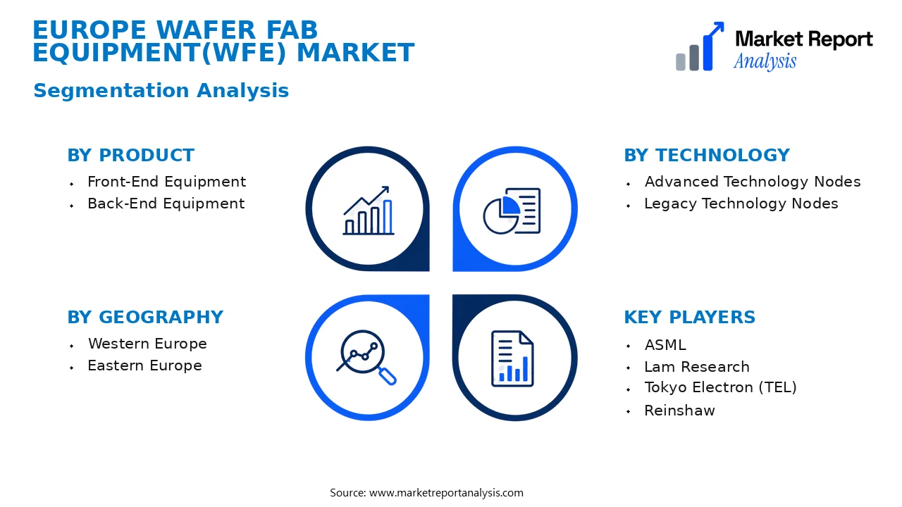
- Product
- Front-End Equipment: This subsegment includes equipment used in wafer fabrication processes such as lithography, etching, and deposition, which are critical for chip manufacturing and reflect advancements in process technology and demand for high-performance semiconductors.
- Back-End Equipment: Comprising equipment involved in wafer testing, packaging, and assembly, this segment supports the completion of wafer production, with demand driven by the growth in electronics and consumer device manufacturing in Europe.
- Technology
- Advanced Technology Nodes: Focused on the latest innovations like 7nm, 5nm, and below, this subsegment illustrates the push for smaller, more efficient chips that meet the high performance and energy efficiency demands of European tech developers and manufacturers.
- Legacy Technology Nodes: This segment serves the existing demand for older, cost-effective fabrication equipment used in mature manufacturing lines, supporting legacy chip production in European semiconductor facilities.
- Geography
- Western Europe: Encompasses major semiconductor hubs like Germany, France, and the UK, characterized by high investment in R&D and advanced manufacturing facilities, thus representing a significant market for WFE equipment.
- Eastern Europe: Focused on regions such as Poland, Czech Republic, and Hungary, this segment is witnessing emerging growth driven by investment incentives, lower operational costs, and expanding electronics manufacturing bases.
Competitive Intelligence
The Europe Wafer Fab Equipment (WFE) market exhibits a competitive landscape characterized by moderate to high concentration, with key players such as Applied Materials, ASML, and Lam Research dominating market share. These firms pursue aggressive business strategies centered on product innovation, technological advancements, and strategic partnerships to strengthen their market positions. Innovation efforts focus on enabling smaller node fabrication and enhancing equipment efficiency, which provides differentiation amidst growing competition. Several companies actively engage in acquisitions to expand technological capabilities and geographic reach, supporting their expansion strategies within Europe's evolving semiconductor ecosystem. R&D investments remain substantial, aimed at developing next-generation equipment with higher throughput and lower defect rates, crucial for meeting advanced node demands. Partnerships with foundries and integrated device manufacturers are vital to co-develop tailored solutions and accelerate market entry. Distinctive competitive differentiation is achieved through advanced precision engineering, proprietary process technologies, and robust after-sales support, reinforcing these companies' positions in this highly specialized domain. Overall, strategic innovation and collaboration are pivotal to maintaining competitiveness in the dynamic Europe WFE market.
Leading Company Profiles
The European Wafer Fab Equipment (WFE) market features a competitive landscape dominated by technological innovation and strategic alliances, with key players continuously enhancing their capabilities to meet increasing demand from semiconductor manufacturers across the region.
- ASML
- Lam Research
- Tokyo Electron (TEL)
- Reinshaw
- AI Klasm
- infineon Technologies
- STMICROELECTRONICS
- AMAT
- Nikon Corporation
- Sunway Technology
ASML
ASML leads the market with its advanced lithography solutions, including EUV and deep UV systems, strategically focusing on process innovation and expanding its global manufacturing footprint to support the increasing demand for more sophisticated chips.
Lam Research
Specializing in wafer fabrication equipment for etching and deposition, Lam Research remains a key innovator, investing heavily in R&D to develop next-generation plasma etch and clean tools for high-volume production environments.
Tokyo Electron (TEL)
Tokyo Electron is recognized for its comprehensive portfolio covering deposition, etch, cleaning, and metrology systems, emphasizing integration of automation and digitalization to enhance manufacturing efficiency and yield in European fabs.
Reinshaw
This company is focusing on high-precision deposition equipment, aiming to provide innovative solutions tailored for advanced nodes, with considerable investments in sustainable manufacturing processes to reduce overall environmental impact.
AI Klasm
AI Klasm concentrates on developing specialized inspection and metrology tools, leveraging AI-driven analytics to improve process control and defect detection, thus supporting the region's push towards smarter fabrication lines.
infineon Technologies
While primarily known for semiconductor manufacturing, infineon is expanding its capabilities in wafer processing equipment, focusing on vertical integration and strategic partnerships to enhance local EU fabrication capacities.
STMICROELECTRONICS
STMicroelectronics invests in advanced WFE for its fabs, prioritizing process scalability and quality enhancement, supported by ongoing collaborations with equipment suppliers to adopt cutting-edge manufacturing technologies.
AMAT
Applied Materials (AMAT) continues to innovate in deposition and etch solutions, emphasizing automation and AI integration, aiming to boost throughput and device performance in the European semiconductor ecosystem.
Nikon Corporation
Nikon advances its lithography systems for wafer fabrication, focusing on extending its technological leadership through R&D and strengthening strategic partnerships to penetrate emerging markets within Europe.
Sunway Technology
Sunway specializes in wafer inspection and metrology equipment, focusing on delivering cost-effective, high-precision tools that meet compliance standards and support the region's semiconductor production growth.
Strategic Business Developments
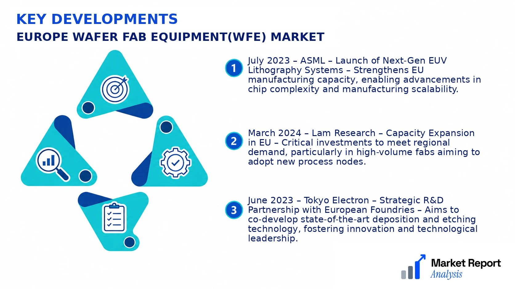
- July 2023 – ASML – Launch of Next-Gen EUV Lithography Systems – Strengthens EU manufacturing capacity, enabling advancements in chip complexity and manufacturing scalability.
- March 2024 – Lam Research – Capacity Expansion in EU – Critical investments to meet regional demand, particularly in high-volume fabs aiming to adopt new process nodes.
- June 2023 – Tokyo Electron – Strategic R&D Partnership with European Foundries – Aims to co-develop state-of-the-art deposition and etching technology, fostering innovation and technological leadership.
- January 2024 – Reinshaw – Acquisition of European Inspection Tech Firm – Enhances product portfolio with advanced metrology solutions, boosting competitiveness in quality control for EU manufacturers.
- September 2023 – AMAT – Opening of New European R&D Center – Focused on AI integration in wafer processing tools, this move aims to accelerate smart manufacturing initiatives across EU fabs.
Frequently Asked Questions
What is the Europe Wafer Fab Equipment(WFE) Market?
The Europe Wafer Fab Equipment (WFE) Market encompasses the manufacturing tools and machinery used in semiconductor wafer fabrication within Europe. It covers equipment for processes like photolithography, etching, deposition, and inspection, crucial for producing advanced semiconductor devices.
What is the current market size of Europe Wafer Fab Equipment(WFE) Market?
The market was valued at approximately USD X billion in 2026, reflecting the growing demand for semiconductor manufacturing capacity across European countries driven by technological advancements and increased investments in chip production facilities.
What factors are driving the Europe Wafer Fab Equipment(WFE) Market?
Key drivers include surging demand for consumer electronics, automotive electronics, and AI chips, alongside government initiatives to bolster domestic semiconductor manufacturing and investments by global OEMs seeking to expand within Europe amid supply chain disruptions.
Which region dominates the Europe Wafer Fab Equipment(WFE) Market?
Germany holds the leading position due to its advanced manufacturing infrastructure and significant investments from European and international semiconductor companies, making it the dominant region in the European WFE landscape.
Which segment is expected to grow the fastest?
The photolithography equipment segment is projected to exhibit the fastest growth, driven by advancements in EUV technology and the increasing production of chips with smaller node sizes, critical for next-generation electronics.
Who are the leading companies operating in the Europe Wafer Fab Equipment(WFE) Market?
Major players include ASML, Nikon, and Ultratech, with other notable companies like Lam Research and Applied Materials also expanding their presence through strategic investments and partnerships in the European region.
Analyst Perspective
The Europe Wafer Fab Equipment (WFE) market is poised for sustained growth through 2034, driven by ongoing technological advancements and increased demand for advanced semiconductors. Long-term market prospects remain favorable, with a focus on automation, higher productivity, and process innovation to meet the specifications of next-generation chips. Emerging opportunities lie in the expansion of Europe’s domestic manufacturing capacity, supported by government incentives and strategic investments in new fabrication facilities, which will foster a more resilient supply chain. Technology evolution will likely emphasize EUV lithography, advanced metrology, and automation tools, positioning firms to capitalize on the move toward smaller node sizes. Regional growth potential is strongest in markets prioritizing localization and technological sovereignty, notably in Germany, France, and the UK. Investment priorities should target R&D, strategic partnerships, and capacity expansion, while navigating high competitive intensity. Long-term, Europe’s WFE market will benefit from an innovation-driven environment, with regional players aligning to global trends, creating a resilient ecosystem for continued expansion.
