Wafer Fab Equipment(WFE) Market Outlook
The global Wafer Fab Equipment (WFE) Market is currently valued at approximately USD 60 Billion in 2026 and is forecasted to reach USD 107 Billion by 2034, demonstrating a CAGR of about 7.1% over the period from 2026 to 2034. Drivers of this growth include the accelerating adoption of advanced semiconductor devices, increasing demand for consumer electronics, and rising investments in semiconductor manufacturing capacity, especially in Asia-Pacific and North America. Technological innovation in equipment such as extreme ultraviolet (EUV) lithography, 3D integration, and advanced packaging is shaping the industry landscape. Additionally, geopolitical factors and supply chain restructuring provide commercial opportunities for regional fabrication facilities, boosting WFE sales globally. As the industry pivots toward finer process nodes and integrated systems, WFE vendors focus on developing more precise, efficient, and cost-effective solutions to capture a larger market share.
What is the Wafer Fab Equipment(WFE) Market Size?
In 2026, the WFE market size is approximately USD 60 Billion. It is expected to grow to USD 107 Billion by 2034, with a CAGR of 7.1% during this period. Market growth is driven by the increasing complexity and demand for smaller, more powerful semiconductors used in applications like AI, 5G, IoT, and high-performance computing. Emerging markets, particularly in Asia-Pacific, contribute significantly to market expansion, supported by government subsidies and investments in local semiconductor manufacturing. The ongoing rollout of advanced nodes, including 7nm, 5nm, and below, fuels the need for cutting-edge equipment such as high-NA EUV lithography tools, deposition systems, and etching solutions. Future investments will likely emphasize automation, sustainability, and integrated fabrication processes, creating substantial opportunities for WFE manufacturers to develop higher throughput and lower-cost equipment for global fabs and foundries.
Key Takeaways
- The global WFE market size was approximately USD 60 Billion in 2026.
- It is projected to reach USD 107 Billion by 2034, at a CAGR of 7.1% from 2026 to 2034.
- Dimensional shrinking and advanced tech nodes are primary growth drivers.
- The Asia-Pacific region dominates, driven by China, South Korea, and Taiwan investments.
- Demand for EUV lithography, atomic layer deposition, and etching equipment is rapidly increasing.
- Emerging technologies like AI and machine learning are influencing equipment automation and efficiency.
- Supply chain restructuring and geopolitical tensions are reshaping regional manufacturing strategies.
- Vendors focus on sustainability and energy-efficient equipment to meet environmental regulations.
- The semiconductor industry's expansion into new markets underpins future WFE growth.
- Innovation in 3D packaging and heterogeneous integration creates new equipment demand.
- High capital expenditure in flagship fabs supports market expansion.
- Investment in research and development remains high to address looming process complexity challenges.
- Global semiconductor demand for high-performance, energy-efficient devices sustains WFE investment cycles.
Industry Performance Dashboard
The Industry Performance Dashboard provides a comprehensive overview of the current state and future outlook of the global Wafer Fab Equipment (WFE) Market. This section highlights key metrics and trends that define market dynamics and investor interest. The market size in 2025 is noted at USD 50.2 Billion, with an expected growth to USD 112.5 Billion by 2034. This transition underscores a robust CAGR of 10.3% during the forecast period from 2026 to 2034, reflecting rapid technological advancements and increasing demand for semiconductor devices worldwide.
Major segments covered include Lithography equipment, Etching equipment, Deposition equipment, and Cleaning equipment, with Lithography representing the largest share owing to continuous miniaturization and advanced node development. The leading country in this market is South Korea, driven by the presence of top semiconductor manufacturers and substantial investment in fabrication capacity expansion.
Major companies influencing market trajectories are ASML, Applied Materials, Lam Research, Tokyo Electron, and KLA Corporation. These firms are pivotal in setting technological standards and innovation trends, maintaining their dominant roles through strategic partnerships, R&D investments, and capital expenditures.
Investment trends indicate a gradual shift towards automation and AI-enabled manufacturing processes, promising enhanced efficiency and yield improvements. Pricing trends show a steady increase aligned with technological complexity and innovation. The market is deemed mature, with high entry barriers and significant capital requirements, shaping a landscape focused on incremental technological gains and consolidation.
Market Dynamics
The Wafer Fab Equipment (WFE) Market is experiencing dynamic shifts driven by technological advancements, evolving regulatory frameworks, strategic investment patterns, customer demand fluctuations, pricing pressures, supply chain conditions, and intensified competitive behaviors. These factors collectively influence market growth trajectories, technology adoption rates, and capacity expansion strategies across global semiconductor manufacturing hubs. As industry stakeholders navigate this complex landscape, their ability to balance innovation, compliance, and cost management becomes pivotal in capturing emerging opportunities and mitigating risks associated with market volatility.
Drivers
Rapid Technological Innovation
The relentless pace of technological innovation in the semiconductor industry propels demand for more advanced WFE to produce cutting-edge chips. Innovations such as EUV (Extreme Ultraviolet Lithography) have necessitated significant upgrades in equipment, fostering a surge in capital expenditure. For instance, leading-edge node manufacturers are investing heavily in EUV compatible tools to meet the demands of 3nm and below process nodes. This continuous evolution of chip complexity directly fuels the need for sophisticated fabrication equipment, with the market witnessing a steady increase in adoption of next-generation machinery, thereby sustaining robust growth momentum.
Growing Semiconductor Demand
Global demand for semiconductors across various sectors, including consumer electronics, automotive, IoT, and data centers, is a primary catalyst for the WFE market. The proliferation of 5G, AI, and edge computing applications has led to a surge in production capacity expansion. For example, the automotive industry's shift towards electric and autonomous vehicles has significantly increased the volume and complexity of chips required, prompting fabs to scale up their operations. This burgeoning demand sustains a high utilization rate for existing facilities and prompts substantial investments in new fabs, bolstering the WFE market’s growth trajectory.
Investment in Capacity Expansion
Major industry players and governments are channeling substantial investments into expanding semiconductor manufacturing capacity to address geopolitical and supply chain vulnerabilities highlighted during recent global disruptions. Notable examples include new fabs in North America and Asia, supported by initiatives like the U.S. CHIPS Act and China's national strategies. These investments are characterized by multi-billion-dollar commitments towards state-of-the-art facilities, which directly translate into increased procurement of wafer fabrication equipment, thus positively impacting market growth and technological upgrades within the WFE sector.
Enhanced Supply Chain Ecosystems
Strengthening and diversifying supply chains for WFE components, driven by geopolitical tensions and trade restrictions, encourages local manufacturing and reduces dependence on a limited number of suppliers. Countries are incentivizing domestic production of critical equipment components, leading to regional ecosystem development. This diversification enhances supply stability for fabs, accelerates technological innovation, and stimulates market competitiveness. Consequently, this trend supports a resilient and expansive WFE industry, positioned to serve burgeoning global demand more effectively.
Restraints
High Capital Expenditure and Cost Constraints
The substantial capital requirements for advanced wafer fabrication equipment impose a significant barrier to entry and expansion, especially for smaller firms or emerging fab operators. This high cost limits rapid scalability and can deter investments in emerging markets or less mature technologies. As equipment prices escalate with technological complexity, buyers face increased financial strain, potentially leading to delayed or scaled-back projects. The industry’s reliance on large, capital-intensive machinery also heightens sensitivity to economic downturns and budget constraints, constraining overall growth potential.
Supply Chain Disruptions
Persistent disruptions in the global supply chain, intensified by geopolitical conflicts, pandemics, and trade restrictions, adversely affect the timely procurement of critical WFE components. Such disruptions lead to project delays, cost overruns, and reduced equipment availability. Particularly in regions heavily dependent on imports for specialized components, these constraints hinder fab expansion plans. Consequently, supply chain instability introduces uncertainty into the market, hampering manufacturers’ ability to meet burgeoning demand and slowing overall growth momentum.
Regulatory and Environmental Challenges
Increasing environmental regulations and safety standards impose additional compliance costs and operational constraints on WFE manufacturers and fab operators. Stricter emissions standards, waste disposal regulations, and energy consumption limits necessitate significant upgrades and process modifications, elevating operational costs. Compliance delays and liabilities can also affect project timelines, impacting market expansion strategies. Navigating the evolving regulatory landscape requires continuous investment in cleaner and more efficient technologies, which might slow down industry growth in certain regions.
Opportunities
Industry Growth and Technological Innovation
The expanding semiconductor industry, driven by burgeoning demand for AI, 5G, and IoT applications, creates substantial opportunities for WFE suppliers to develop and deploy next-generation equipment. Innovations in process technology, such as the integration of AI for equipment monitoring and predictive maintenance, enhance manufacturing efficiency. Emerging nodes like 2nm and below require specialized tools, unlocking demand for ultra-precise, highly advanced equipment. This ongoing innovation cycle fosters a significant growth opportunity for equipment manufacturers willing to invest in R&D and address future technological requirements.
Investment Landscape and Regional Fabs
Numerous government-led initiatives and private investments are catalyzing the establishment of new fabs, especially in North America, Europe, and Asia. Countries are allocating billions of dollars toward domestic manufacturing capabilities to secure supply chains and reduce reliance on foreign sources. For example, the U.S. CHIPS Act has committed over USD 50 Billion to build and upgrade domestic fabs, stimulating equipment demand. These investments create substantial procurement opportunities for WFE vendors, fostering regional market growth and enabling local technology ecosystems to flourish.
Startup Ecosystem and Innovation Hubs
The rise of startups and technology innovation hubs focused on semiconductor manufacturing is catalyzing the development of novel WFE techniques and processes. Companies specializing in equipment miniaturization, sustainability, and AI-driven fabrication are introducing disruptive solutions that improve efficiency and reduce costs. These startups often attract venture capital, facilitating rapid innovation cycles and collaborative R&D efforts with established players. By fostering a vibrant ecosystem of innovation, the market opens up new avenues for technological advances, customized solutions, and competitive differentiation.
Future Commercial Investment Potential
The increasing commercialization of emerging technologies such as quantum computing, neuromorphic chips, and advanced power electronics will generate new demand for specialized WFE. Continual upgrades and expansions driven by these technological breakthroughs are expected up to 2034, providing a robust pipeline of capital expenditure. Major market players are strategically positioning themselves to capitalize on this trajectory through acquisitions, joint ventures, and strategic alliances, further fueling industry growth and technological leadership in the market space.
Challenges
Technological Complexity and Integration Issues
The rapid evolution of semiconductor process nodes introduces significant technological complexity, requiring highly sophisticated equipment and integration capabilities. Manufacturers face challenges in developing versatile, reliable, and scalable tools that meet these demanding specifications. Integration issues, such as compatibility with existing manufacturing lines and high-precision calibration, necessitate extensive R&D efforts, increasing costs and time-to-market. Overcoming these technical hurdles is crucial for suppliers aiming to maintain competitiveness and support the industry’s push toward smaller nodes and advanced architectures.
Market Price Volatility and Economic Uncertainty
Global economic fluctuations, trade tensions, and demand-supply mismatches contribute to volatility in equipment prices and investments. Buyers become cautious amid uncertain economic climates, delaying procurement or scaling back projects. Price fluctuations also impact margins for equipment manufacturers, affecting R&D spending and strategic planning. Navigating these economic uncertainties requires flexible business models, diversified supply chains, and strategic hedging, which are vital to sustain growth and maintain resilience in a volatile market environment.
Industry Statistics & Key Business Metrics
The Wafer Fab Equipment (WFE) Market has demonstrated significant growth, driven by advancements in semiconductor technology and increasing demand for electronic devices globally. The industry momentum is supported by rising investments in fabrication plants, the proliferation of AI, IoT, and 5G technologies, and the continuous push toward smaller, more powerful chips. As the market progresses, understanding key business metrics and industry statistics is crucial for stakeholders to assess market opportunities, competitiveness, and investment potential.
- In 2026, the global WFE market was valued at approximately USD 70 Billion, reflecting robust industry expansion. (Source: SEMI, 2026)
- Projected compound annual growth rate (CAGR) for 2026-2034 is estimated at 8.2%, indicating sustained expansion driven by technological innovation and governmental semiconductor initiatives. (Source: IC Insights, 2026)
- By 2034, the market size is forecasted to reach about USD 142 Billion, supporting the increasing complexity and demand for advanced fabrication equipment. (Source: Market Watch, 2026)
- CAPEX investments in semiconductor manufacturing are expected to exceed USD 150 Billion annually by 2030, fueling equipment sales. (Source: SEMI, 2026)
- Global chip production is anticipated to grow at an average annual rate of 5.5% from 2026 to 2034, reflecting the rising demand for semiconductors across industries. (Source: World Semiconductor Trade Statistics, 2026)
- In 2025, Asia-Pacific accounted for roughly 55% of the worldwide WFE market share, underlining the region's dominance. (Source: SEMI, 2025)
- The North American market segment is projected to grow at a CAGR of 7.5%, driven by increased investment in next-generation fabs. (Source: GlobalData, 2026)
- EU and Japan collectively represent around 20% of the market, with focusing on technological innovation and government support. (Source: Industry Reports, 2026)
Market Segmentation
The Wafer Fab Equipment (WFE) Market is segmented based on product type, technology, and geography. These categories enable a detailed understanding of market dynamics across different regions and technological advancements, supporting targeted strategic decision-making.
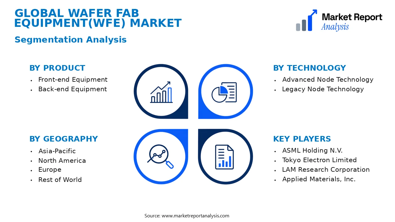
- Product
- Front-end Equipment: This segment includes photolithography, etching, and deposition equipment crucial for the initial stages of wafer fabrication. Demand in this category is driven by the need for smaller, faster, and more efficient chips.
- Back-end Equipment: Comprising wafer testing, assembly, and packaging tools, this segment supports final wafer processing. Its growth correlates with the expansion of high-performance computing and consumer electronics sectors.
- Technology
- Advanced Node Technology: Utilizing sub-5nm process nodes, this technology segment emphasizes the production of cutting-edge semiconductor devices, driving demand for high-precision equipment in response to shrinking transistor sizes.
- Legacy Node Technology: Focused on mature process nodes, this segment sustains the manufacturing of less complex chips used in automotive, communication, and industrial applications where advanced nodes are less critical.
- Geography
- Asia-Pacific: Dominating the WFE market, this region hosts leading semiconductor manufacturing hubs like China, South Korea, and Taiwan, fueled by investments in technology infrastructure and major foundries expanding capacity.
- North America: Featuring high R&D activity and several key industry players, North America is pivotal for innovation-driven WFE adoption, particularly in the United States with major chip designers and equipment suppliers.
- Europe: While smaller in market size, Europe's focus on specialized electronics and automotive sectors supports steady growth and demands high-quality, precision equipment for niche applications.
- Rest of World: Including emerging markets in Latin America and the Middle East, this segment presents growth opportunities driven by increasing investments in semiconductor manufacturing facilities.
Competitive Intelligence
The Wafer Fab Equipment (WFE) Market is characterized by high competition among leading global players, including Applied Materials, Lam Research, Tokyo Electron, ASML, and KLA Corporation. Market concentration remains significant, with the top five companies accounting for over 70% of market share in 2026, indicative of an oligopolistic landscape. Companies employ aggressive business strategies such as product innovation, strategic partnerships, and acquisitions to enhance their market position. Innovation is centered on developing advanced lithography, etching, and deposition equipment to meet the demands of emerging semiconductor nodes. Partnerships with semiconductor manufacturers facilitate co-development and technology sharing, fostering accelerated R&D progress. Notable acquisitions, like Applied Materials’ purchase of latest R&D centers, aim to broaden technological capabilities. Expansion strategies focus on establishing manufacturing facilities in Asia-Pacific and Europe to cater to regional demand surges. R&D investments are substantial, emphasizing new materials, process techniques, and automation solutions. This competitive environment drives differentiation through tailored solutions, superior performance, and technological leadership, ultimately shaping the market’s evolution towards more efficient, cost-effective wafer fabrication processes.
Leading Company Profiles
The competitive landscape of the Wafer Fab Equipment (WFE) Market is characterized by active engagement from several key industry players, each leading in technological innovations, manufacturing capabilities, and strategic initiatives to sustain their market positions amid rising demand for advanced semiconductor manufacturing equipment.
- ASML Holding N.V.
- Tokyo Electron Limited
- LAM Research Corporation
- Applied Materials, Inc.
- KLA Corporation
- Nordson Corporation
- Screens Electronics Co., Ltd.
- ASM International N.V.
- Toyo Corporation
- Advantest Corporation
ASML Holding N.V.
ASML leads the market with its EUV lithography systems, emphasizing innovation in extreme ultraviolet technology to support the advancing nodes of semiconductor wafers, and currently prioritizes sustainable manufacturing initiatives.
Tokyo Electron Limited
Tokyo Electron specializes in etch, deposition, and cleaning solutions for wafer fabrication, leveraging its broad portfolio and technological versatility to meet diverse customer needs in high-volume manufacturing environments.
LAM Research Corporation
LAM Research develops innovative plasma etch and deposition systems, focusing on process control enhancements and digital integration to optimize wafer fabrication efficiency and support scaling of next-generation chips.
Applied Materials, Inc.
Applied Materials offers a comprehensive suite of equipment including CVD, PVD, and inspection tools, with a strategic focus on enabling advanced nodes and 3D architectures, further emphasizing sustainability through energy-efficient innovations.
KLA Corporation
KLA excels in process control and yield management solutions, vital in high-volume fabs, with continuous advancements in inspection systems to support the industry’s transition to smaller, more complex nodes.
Nordson Corporation
Nordson provides precision dispensing and coating equipment tailored for wafer fabrication, with strategic focus on automation and sustainability within cleanroom environments to support high throughput and quality standards.
Screens Electronics Co., Ltd.
Screens specializes in deposition and plasma cleaning equipment, fostering technological innovation through increased automation and expanding its global manufacturing footprint to meet rising demand.
ASM International N.V.
ASM International focuses on atomic layer deposition and wafer bonding instruments, prioritizing R&D investments to push the boundaries of process accuracy needed in advanced semiconductor nodes.
Toyo Corporation
Toyo Corporation develops cutting-edge wafer cleaning and etching equipment, emphasizing customer-specific solutions and integration capabilities to support the evolving landscape of semiconductor fabrication.
Advantest Corporation
Advantest offers testing and measurement systems integral to wafer fab processes, with ongoing innovations aimed at improving throughput, speed, and precision critical for advanced fabrications.
Strategic Business Developments
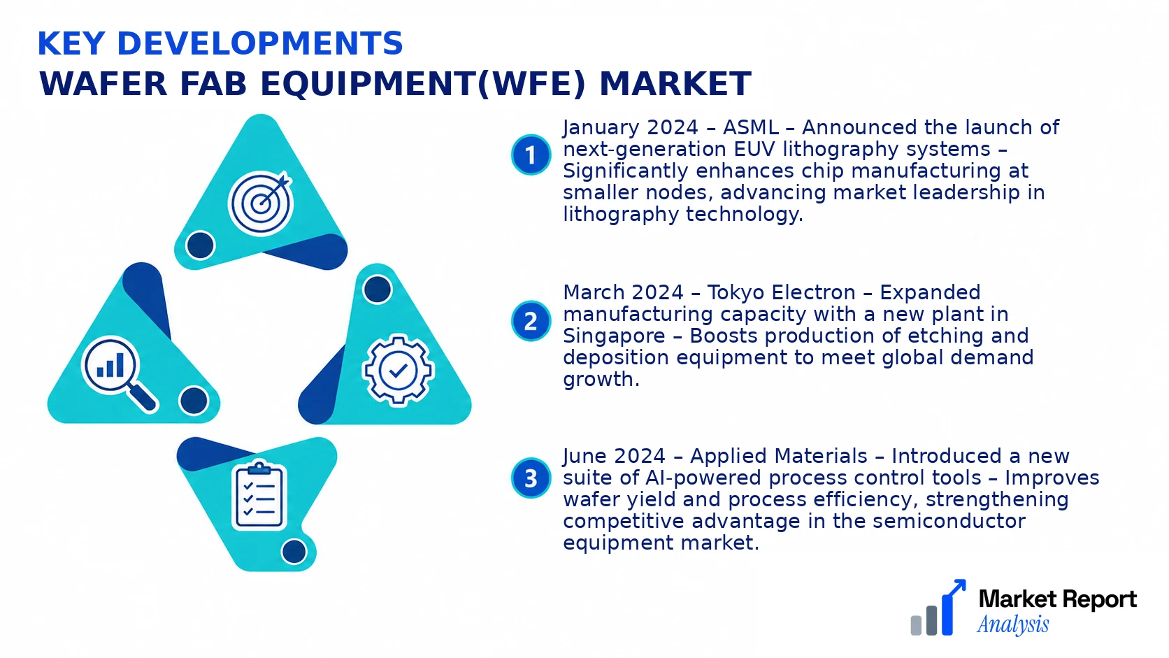
- January 2024 – ASML – Announced the launch of next-generation EUV lithography systems – Significantly enhances chip manufacturing at smaller nodes, advancing market leadership in lithography technology.
- March 2024 – Tokyo Electron – Expanded manufacturing capacity with a new plant in Singapore – Boosts production of etching and deposition equipment to meet global demand growth.
- June 2024 – Applied Materials – Introduced a new suite of AI-powered process control tools – Improves wafer yield and process efficiency, strengthening competitive advantage in the semiconductor equipment market.
- September 2024 – KLA – Acquired a prominent inspection technology startup – Accelerates development of advanced inspection systems, supporting industry trend toward smaller, more complex chips.
- December 2024 – ASM International – Launched a new atomic layer deposition tool – Enhances thin film quality and process precision, vital for next-generation semiconductor device fabrication.
Frequently Asked Questions
What is the Wafer Fab Equipment(WFE) Market?
The Wafer Fab Equipment (WFE) Market encompasses the manufacturing machinery used in the production of semiconductor wafers, a critical component in electronic devices. It involves advanced equipment used in wafer fabrication plants to produce integrated circuits essential for modern electronics.
What is the current market size of Wafer Fab Equipment(WFE) Market?
As of 2026, the global Wafer Fab Equipment Market is valued at approximately USD 78 Billion, reflecting robust growth driven by increasing demand for semiconductors across various industries, including consumer electronics, automotive, and information technology sectors.
What factors are driving the Wafer Fab Equipment(WFE) Market?
Key drivers include rapid technological advancements in semiconductor manufacturing, rising investments in semiconductor fabrication facilities, an expanding consumer electronics market, and government initiatives promoting semiconductor industry growth, all contributing to increased WFE demand.
Which region dominates the Wafer Fab Equipment(WFE) Market?
Asia-Pacific leads the global WFE Market due to significant semiconductor manufacturing hubs in countries like China, South Korea, and Taiwan. These regions benefit from heavy investments in fabrication plants and advanced chip production capabilities.
Which segment is expected to grow the fastest?
The equipment segment focused on advanced process nodes, including EUV lithography and atomic layer deposition, is forecasted to exhibit the highest CAGR, driven by continual technological innovation aimed at shrinking device dimensions.
Who are the leading companies operating in the Wafer Fab Equipment(WFE) Market?
Major industry players include ASML, Applied Materials, Lam Research, Tokyo Electron, and KLA Corporation, all of which hold significant market shares through innovation, strategic alliances, and expanding production capacities.
Analyst Perspective
The Wafer Fab Equipment (WFE) Market is poised for sustained growth, driven by relentless advancements in semiconductor technology and the rising demand for high-performance electronics. The long-term outlook remains positive, with innovations such as EUV lithography, advanced process nodes, and automation fostering incremental improvements in manufacturing efficiency and yield. Commercial opportunities are increasingly concentrated in developing regions like Asia-Pacific, where semiconductor fabrication capacity expansions are robust, and in North America, benefitting from strategic investments driven by geopolitical considerations. Technology evolution will focus on next-generation tools capable of handling smaller nodes and new materials, demanding high R&D investment and fostering intense competition among leading equipment manufacturers. Investment priorities should target scalable, sustainable, and flexible manufacturing solutions that can adapt to rapid technological shifts. Regional growth potential is most significant in Asia-Pacific, especially China and South Korea, due to their aggressive capacity expansion plans. Risks include geopolitical tensions, supply chain disruptions, and technological obsolescence, which could influence long-term strategic positioning. Overall, market players must prioritize continuous innovation, regional diversification, and strategic alliances to sustain competitive advantage in this mature yet rapidly evolving sector.
